Wafer Bumping 101l6e
This document was ed by and they confirmed that they have the permission to share it. If you are author or own the copyright of this book, please report to us by using this report form. Report 2z6p3t
Overview 5o1f4z
& View Wafer Bumping as PDF for free.
More details 6z3438
- Words: 212
- Pages: 2
Wafer Bumping Wafer bumping services are offered as a preparatory step for flip-chip bonding or as bumping service alone. The types of solder bumping available include high lead solder, eutectic solder and lead free solder. Lead free bump, which is composed of tin-silver alloy, can meet the WEEE directives. Additionally, it can eliminate alpha particle sources. Fujitsu's solder bumping service is currently offered for 6”and 8”wafers, and soon 12" wafers. Using advanced technology fabrication, Fujitsu manufactures 11,000 bumps on a die with 120µm bump pitch with lead free solder, and a 100µm bump pitch. Cross section of solder bump
Solder Ball
Barrier Metal Ni (plated) Cu (sputtered) Ti (sputtered)
Silicon
AI Pad
ivation
Cross section of electroless Ni UBM and AP- bump Solder Bump
AI Pad ivation
[UBM] Nickel
• • • • • 5
Fujitsu Microelectronics America, Inc.
Industry's most extensive experience Lead-free and other innovative bumping solutions Copper wiring redistribution services Tightest bump pitch Single die bumping capability
Wafer Bumping Fine-pitch bump
Bump pitch:100um Bump height: 50um
Solder Bumping Process Flow 1. UBM sputtering
Ni (sputter)
ivation
2. Resist patterning for plating
Resist Ti (sputter)
3. Ni plating
4. PbSn Plating
PbSn (plating) Ni (plating)
Pad metal
5. Resist removing
6. Cu/Ti etching
7. Bump shaping
Advanced Packaging Services
6
Related Documents c2h70

Wafer Bumping 101l6e
March 2023 0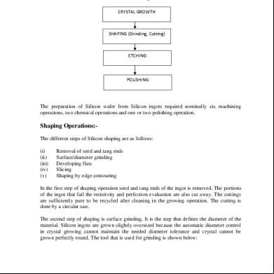
Wafer Preparation 2t3w2n
October 2019 74
Resepi Wafer 6w716l
December 2019 51
What Is Bumping Clearance w6w1j
October 2021 0
Silicon Wafer Fabrication u1r1z
July 2021 0
Probe On-wafer Diodes 382837
August 2021 0More Documents from "Safalsha Babu" 2r131u

Wireless Charging Of Mobile Phones Using Microwaves 4w274l
December 2019 39
Wireless Heart Attack Detector With Gps 92325
October 2021 0
Dry_ice 245771
August 2020 0
Wafer Bumping 101l6e
March 2023 0
Dlda - M_09 1j2j3d
December 2019 94