Silicon Wafer Fabrication u1r1z
This document was ed by and they confirmed that they have the permission to share it. If you are author or own the copyright of this book, please report to us by using this report form. Report 2z6p3t
Overview 5o1f4z
& View Silicon Wafer Fabrication as PDF for free.
More details 6z3438
- Words: 575
- Pages: 24
Silicon and Wafer Preparation Lyndon Mark P. Olaguera PS147: Physical Electronics
OBJECTIVES At the end of this lesson, the student should be able to: 1. describe how the raw silicon is refined into semiconductorgrade silicon. 2. explain the crystal structure and growth method for producing mono-crystalline silicon. 3. outline and describe the basic process steps for wafer preparation, starting from a silicon ingot and finishing with a wafer. 4. explain what epitaxy is and why it is important for wafers.
Semiconductor Grade Si Pure silicon—used to minimize micro-defects at the atomic level of the silicon that are detrimental to semiconductor performance. Semiconductor grade Si(SGS)—highly refined silicon >>also known as electronic grade silicon
Semiconductor Grade Si
Source: Semiconductor Manufacturing Technology by Michael Quirk, Julian Seda, 2001
Siemens Process Silicon produced by this process does not have atoms arranged in a desirable crystal order.
Source: Semiconductor Manufacturing Technology by Michael Quirk, Julian Seda, 2001
CRYSTAL STRUCTURE CRYSTAL>>a solid material that has an ordered, repeatable three dimensional pattern over a long range of many atoms.
Source: Semiconductor Manufacturing Technology by Michael Quirk, Julian Seda, 2001
CRYSTAL STRUCTURE Amorphous Materials >>non crystalline solids that lack a repetitive structure and demonstrate structural disorder at the atomic level. E.g. Plastic Source: Semiconductor Manufacturing Technology by Michael Quirk, Julian Seda, 2001
CRYSTAL STRUCTURE Unit Cell >>the simplest arrangement of atoms that, when repeated in a three dimensional framework gives the crystal structure.
Source: Semiconductor Manufacturing Technology by Michael Quirk, Julian Seda, 2001
CRYSTAL STRUCTURE
http://2.bp.blogspot.com/-B-6gSM0wsXw/UC_bwvm7ooI/AAAAAAAABAw/1y1TIhYkc/s1600/seven.pnghttp://2.bp.blogspot.com/-B6gSM0wsXw/UC_bwvm7ooI/AAAAAAAABAw/1y1TIhYkc/s1600/seven.pnghttp://2.bp.blogspot.com/-B6gSM0wsXw/UC_bwvm7ooI/AAAAAAAABAw/1y1TIhYkc/s1600/seven.pngv
CRYSTAL STRUCTURE
Source: Semiconductor Manufacturing Technology by Michael Quirk, Julian Seda, 2001
CRYSTAL STRUCTURE Within a crystal structure, unit cells are tightly packed, therefore, share atoms. Sharing of atoms– this is how unit cells build up into a cohesive crystal lattice structure. FCC unit cell—four shared atoms. Silicon crystal—Four shared and Four unshared (four atoms inside the cubic structure) Source: Semiconductor Manufacturing Technology by Michael Quirk, Julian Seda, 2001
POLY-CRYSTAL and MONOCRYSTAL Poly crystal—the unit cells are not in a regular arrangement. Silicon produced from the semiconductor grade purification process— poly-silicon. Mono-crystals—if unit cells are neatly arranged in a three dimensional, repeatable manner.
Source: Semiconductor Manufacturing Technology by Michael Quirk, Julian Seda, 2001.
REQUIREMENTS for Si Wafer Processing
Pure Mono-crystalline WHY?? 1. Repeatable units provide the desirable electrical and mechanical properties
CRYSTAL ORIENTATION
(100)– common for MOS devices, GaAs devices. (111)—bipolar devices (tighter packing density)
Source: Semiconductor Manufacturing Technology by Michael Quirk, Julian Seda, 2001.
MONOCRYSTAL SILICON GROWTH Crystal Growth—process of converting the polysilicon chunks of SGS into a large monocrystal of Si. INGOT—grown silicon monocrystal. Czochralsky Method (CZ)--Most commonly used technique for growing monocrystal ingots.
Source: Semiconductor Manufacturing Technology by Michael Quirk, Julian Seda, 2001.
MONOCRYSTAL SILICON GROWTH Objectives of the pull process: Replicate the seed structure while obtaining dopant uniformity Achieving the correct ingot diameter Limiting the introduction of impurities
Parameters affecting the growth process: 1. Pull rate 2. Crystal rotation 3. //Temperature
DOPING
Adding impurities to obtain the desired resistivity Resistivity of pure silicon =2.5x10^5 ohm-cm
FLOAT ZONE METHOD Produces a silicon monoscrystal ingot which significantly lower oxygen content. Produces ingots with smaller diameters.
WAFER DIAMETERS
WAFER PREPARATION
SHAPING OPERATIONS End Removal Diameter Grinding Wafer Flat or Notch
Source: Semiconductor Manufacturing Technology by Michael Quirk, Julian Seda, 2001.
WAFER IDENTIFYING FLATS
Source: Semiconductor Manufacturing Technology by Michael Quirk, Julian Seda, 2001.
WAFER SLICING
http://www.pveducation.org/node/496
WAFER LAPPING
http://www.microchemicals.com/s/pics/wafer_lapping_polishing.jpg
Related Documents c2h70

Silicon Wafer Fabrication u1r1z
July 2021 0
Silicon Wafer Preparation f57u
December 2019 41
Solar Cells - Silicon Wafer-based Technologies 26562
November 2021 0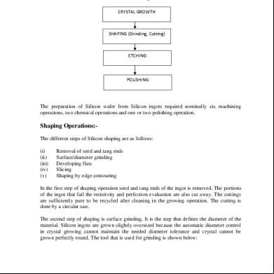
Wafer Preparation 2t3w2n
October 2019 74
Resepi Wafer 6w716l
December 2019 51
Wafer Bumping 101l6e
March 2023 0More Documents from "Jomel U. Maroma" 1a1m1u
Silicon Wafer Fabrication u1r1z
July 2021 0
Kaidah Kebahasaan Teks Laporan Hasil Observasi 52706w
April 2022 0
December 2021 0

Sistema De Control Pid Para Un Pendulo Oscilante 5v2w4d
April 2020 8
1993 Alyssa Valdez Was Born On June 29 6fk6x
January 2022 0