Otn Framer Project Book 4l215z
This document was ed by and they confirmed that they have the permission to share it. If you are author or own the copyright of this book, please report to us by using this report form. Report 2z6p3t
Overview 5o1f4z
& View Otn Framer Project Book as PDF for free.
More details 6z3438
- Words: 6,864
- Pages: 54
Bar Ilan University School of Engineering VLSI Lab
OTN Framer Netanel Gonen Maayan Morali Academic Advisor: Prof. Shmuel Wimer Instructor: Mr. Moshe Doron
Final Fourth Year Project Computer Engineering
Table of Content Introduction……………………………………………...………………...……..……..4 Theoretical Background……………………………………………...……..…..…5 Goals………………………………………………………………..………….…..……..11 General Structure……………………………………………………..………….…12 TOP module……………………………………………………………………………13 The Transmitter ……………….………..…………………………..……….……..16 Transmitter modules TopTx……………….………………………………………………..…..…..…17 DataPreparation……………..…………………………………………..……..…..…20 Tx_Mux…………………………..………………………………………………...…..…22 FrameCreating………………..………………………………………………...…..…24 OutMux…………………………..…….…………………………………………..…..…26 Scrambler………………………..………………………………………………..…..…27
The Receiver………….………….………..…………………………..…..………..29 Receiver modules Rx_top……………….…………………………………………………..…..…32 OTN Framer
Page 2
Data_reception…….…………………………………………………..…..…34 Aligner…….……………………………………………………………..…..…36 De-scrambler…….……………………………………….…………….…..…..…39 Data_arrange…….…………………………………….……………….…..…..…40 Demux…….……………………………………….…………….…………..…..…43
Hardware environment……….………………………….……………………45 Software environment……….…………………………………………………46 Implementation Stages……….…………………………………………………48 Challenges and Solutions.…………………………………………...…………49 Future Ideas.……………………………………………………………...…………51 Summary.………..………………………………………………………...…………52 Bibliography.………..…….……………………………………………...…………53
OTN Framer
Page 3
Introduction Due to the large scale globalization process active nowadays, information exchange has become a critical issue, requiring the elaboration of faster, flexible and reliable computer networks. The migration of network technologies to faster protocols (Gigabit / 10 Gb Ethernet) forces the utilization of optical fiber links in both local (LAN) and metropolitan (MAN) network backbones. OTN (Optical Transform Network) is the only standard capable of transporting 10Gb entirely (and this is the reason we use it). In this project we implement the OTN Framer, when our main goal is data transporting at the rate of 10Gbps. In our implementation there are four data sources and four data destinations. The Framer acts also as a Data Router, operating under Network Management supervision. Each source can be routed to any destination. The implementation is based on the structure of the data units – Multiframes. Each Multiframe contains up to 256 frames. The frame has 4 rows of 4080B each, and contains 3 main parts: Headers – first 16B of the row, contain data of routing, monitoring and structure. Data – data from the sources. FEC – Forward Error Correction. The OTN Framer Consists of: Aligner – Each frame has a sequence in its first 6B (FAS = Frame Aligner Sequence) which indicates a beginning of a new frame. The Aligner recognizes that sequence. Data multiplexing – the data coming from the 4 sources is multiplexed before transmission Scrambler – the frames data (all except the FAS) is scrambled and transmitted. The receiver also has a scrambler – in order to Descramble the data it receives. Frames building – the frames are built and consist mainly of the sources data, but the framer must add the Headers and FEC in order to conform to the ITU-T G.709 standard. The receiver should use the headers and FEC and move the correct data to the appropriate destinations. OTN Framer
Page 4
Theoretical Background The need for faster and improved data transmission led to utilization of optical fiber links. As optical component technology has improved, it has become possible to increase the traffic sent over a fiber by sending multiple signals, each on its own wavelength, rather than increasing the rate of a single signal Such multiplexing is referred to as wavelength-division multiplexing (WDM). The Optical Transport Network (OTN) is a network using the ITU-T Rec. G.709 standard for Wavelength Division Multiplexed (WDM) signals, which is lowering the cost of the network. However, the main characteristic of the OTN standard is the presence of an error correction structure, based on the Reed-Solomon(255, 239) algorithm. This structure may correct up to 128B in a burst for each frame, enabling the use of longer optical links. The OTN Protocol The ITU-T is a branch of the International Telecommunication Union (ITU) responsible for analyzing and organizing groups to study and create recommendations for the telecommunication field. The Optical Transport Network (OTN) standard is described in the G.709 ITU-T recommendation, which defines an OTN interface as a set of elements for optical networks capable of providing transporting functionality, multiplexing, routing, management and supervision of optical channels. The OTN interface must have the ability to carry signals from different types of clients, as shown in the Figure:
OTN Framer
Page 5
The OTN frame is composed of 4 lines of 4080 bytes, and divided to three main blocks: Overhead (16 bytes), Payload (3808 bytes) and FEC (256 bytes). The OTN transmission does not follow the logic structure of the frame. It is transmitted column by column as depicted in the Figure:
The OTN standard uses clock regeneration hardware on its receivers, therefore, long sequences of “0”s or “1”s can compromise the clock regeneration process and should be avoided. To avoid those long sequences, OTN transmitters use a scrambling process on the OTN frames before transmission. OTN Framer
Page 6
Scrambler The scrambling process operates conceptually as a Linear Shift (LFSR), using the generating polynomial
.
The output of the scrambling process is added to each bit of the multiframe.
Scrambling is applied after the FEC calculation for all multiframe bytes with the exception of the FAS (Frame Alignment Signal) bytes. This process is symmetric, i.e., the same process used for scrambling the transmission signal, is used during the receiving process to obtain the original descrambled signal. In the OTN Framer project the implementation of the scrambling is performed in one clock cycle, by using 48 XOR gates, when the values were pre-calculated by Matlab and saved in a file – ‘Scrambler_ROM.coe’. The ROM includes this file, and the scrambler uses one value each time – and XORs it with the unscrambled data. Recommendation G.709 defines the OTN multiframe which contains 4 frames (4080 bytes lines, totalizing 16320 bytes). The OTN multiframe is organized in lines, and is composed by the overhead, payload and FEC for each line. The OTN multiframe is transmitted line by line.
OTN Frame Structure
OTN Framer
Page 7
The 3 main parts in the frame are: Headers Payload FEC
Headers:
FAS: The FAS includes the 6 first bytes of a multiframe. It consists of the sequence “F6F6F6282828”. The receiver has a framer which contains 48 comparators comparing the receiving data and this sequence, when equality means a beginning of a new data stream.
MFAS (Multi-Frame Alignment signal): The value of the MFAS byte is incremented each frame providing, thereby a 256 ( ) frames on each multi-frame.
OTU (Optical Channel Transport Unit): The OTU overhead provides supervisory functions to the OTU terminal points. It consists of: three bytes Section Monitoring (SM), a two-byte General Communication Channel (GCC0), and two bytes reserved (RES) for future use.
GCC0:
OTN Framer
Page 8
We used 5 bits (LSB) of these 2B for routing data. For 4 data sources and destinations there are 24 optional combinations of source-destination. Therefore, we need 5b for routing.
ODU overhead: The ODU information structure provides tandem connection monitoring (TCM), end-to-end path supervision, and client signal adaptation via the optical channel payload unit (OPU). The path monitoring (PM) field in the ODU has a similar structure and function to the section monitor field in the OTU overhead.
The ODU also defines six fields for TCM. TCM enables a network operator to monitor the error performance of a signal transiting from its own network ingress and egress points. The six TCM fields provide for tandem connection monitoring in a variety of network configurations, and can cope with nested, overlapping and cascaded topologies, as shown in the figure:
Two two-byte general communications channel fields, GCC1 and GCC2, are defined in row 4 columns 1 to 4. These bytes provide a clear channel connection between ODU termination points. The format of the data carried
OTN Framer
Page 9
in this channel is not defined. The main purpose of these bytes is to carry operator management data. Two fields (RES) are reserved for future standardization and are located in row 2 columns 1-3 and row 4 columns 9-14. These bytes are normally set to all zeros. Finally, a two-byte experimental (EXP) field is defined for experimental purposes. This field will not be subject to future standardization.
Payload
OPU Payload: The OPU overhead is added to the OPU payload and contains information to the adaptation of client signals. The justification control (JC) bytes are used to control the negative justification opportunity (NJO) or positive justification opportunity (PJO). The mapping process generates the JC, NJO and PJO values respectively. The payload structure identifier (PSI) field is defined to transport a 256-byte message aligned with the OTU MFAS. FEC
FEC ( Forward Error Correction): The FEC scheme used in the ITU-T G.709 standard is a Reed-Solomon RS (255,239) code. For every 239 bytes of data, 16 bytes (255-239=16) of data are added for error detection and correction. Before FEC processing, each OTU row is separated into 16 sub rows, in order to increase burst error performance. Each FEC encoder/decoder processes one of these sub-rows. The FEC data bytes are calculated over the 239 information bytes of each sub row and transmitted in the last 16 bytes of the same sub-row. The RS (255,239) code can correct up to 8 symbol errors in the code word when
OTN Framer
Page 10
used for error correction. It can also detect 16 symbol errors in the code word when used for error detection only. In this project, the FEC was not implemented due to lack of time and based on the fact that in a 10Gb rate the FEC is not mandatory.
Goals Optical Transport Network (OTN) protocol is a new network protocol employing the edge of technology making data transfer faster and more reliable. As such, it requires complex hardware and software implementation. The main goal of our project: deg an Optical Transport Network (OTN) Framer – A network element responsible for analyzing and processing OTN frames at the client side according to the ITU-T advance protocol G.709. In thisproject we constructed the Verilog code of the protocol algorithm and used this implementation on the Virtex 6 FPGA (by Xilinx). We tested and simulated the code in order to get a correct implementation of both transmitter and receiver. Our project consisted of the following stages: 1. Protocol Learning – Reading and understanding the complex protocol of the ITU-T G.709. The basis for the project was the fundamental understanding of the Optical Transport Network protocol documentation. As a starting point we began researching network concepts including preceding technologies, OTN Framer
Page 11
the SONET/SDH optical protocol used worldwide. We have come to learn that the two technologies are closely related and that the OTN is an enhancement of the aforementioned SONET/SDH. 2. Studying the FPGA Development boards available and choosing the most suitable one among them. 3. Verilog Learning – Reading tutorials, writing and learning code examples. 4. Code Implementation– Creation of the system consisting of Transmission and reception, using the Optical Transport Network Protocol. 5. Simulating and checking the code in the tools: SimVision (Cadence), ISE (of Xilinx). 6. FPGA burn - burning the Virtex 6 FPGA, located on the Xilinx ML-605 Board, with the code, finish the project‘s presentation.
OTN Framer
Page 12
General Structure
OTN Framer
Page 13
TOP module Inputs
Din1 (48bit) -
System input from port1.
Din2 (48bit) -
System input from port2.
Din3 (48bit) -
System input from port3.
Din4 (48bit) -
System input from port4.
Routing info -
The routing input. Which input should go to which output.
Clk -
System clock
Clk_sampling -
the sampling clock.
En -
system enable.
Nrst_top -
system active low reset.
Outputs
Dout1 (64bit) -
data out to port1.
Dout2 (64bit) -
data out to port2.
Dout3 (64bit) -
data out to port3.
Dout4 (64bit) -
data out to port4.
Valid_out -
Flag indicating a new data is in the output.
OTN Framer
Page 14
Description: The OTN Framer Top Module Gets data from 4 sources (ROMs) and outputs the data to 4 destinations (RAMs). It contains 2 modules: TopTx and rx_top. Each module represents a different part in the system – the transmitter and the receiver. The transmitter transmit the scrambled data and the receiver receive the data, desrambles it and put it in RAMs. The top module contains 2 modules: 1. TopTx 2. rx_top
OTN Framer
Page 15
OTN Framer
Page 16
The Transmitter In the OTN Framer Project, the Transmitter is the start point for the data. Every 4 cycles the Transmitter samples 48bit x 4 of data from its inputs, and every cycle it transmits 48bits to the Communication Line. It adds to each transmitted frame a Start-of-Frame bits sequence, multiplex the data from the 4 data sources, adds headers and FEC (Forward Error Correction, after calculation of the FEC), scrambles the data, and transmits the data. Basic assumptions The FEC in our project will be set to its default value 0. According to the STD, only in 100Gbps rate, FEC usage is mandatory. The data is transmitted in full frames (no partial frames in the system). Data Flow The data flow works as flowing: 1. Sample 48bits x 4 from the input data each 4 clk cycles. 2. Create frames: -
Add headers (16Bytes on each row in the frame).
-
Multiplex data from 4 data sources (3808Byes on each row).
-
Add FEC bytes (256Bytes on each row).
3. Scramble each 6Bytes of data 4. On each Start-of-Frame add the sequence ‘F6F6F6282828’. 5. Transmit the data (48Bytes on each cycle).
OTN Framer
Page 17
Transmitter modules Tx module is divided to several smaller modules. Each one of them has specific function. TopTx Inputs:
Clk – System clock. clk_sampling System sampling data clock. nrst – System active low reset. en – System enable FECenable – FEC enable Routing (5 bits) Routing data (there are 4!=24 option of sourcedestination combination) data_in1 (48 bits)- Raw data from source 1 data_in2 ( 48 bits)- Raw data from source 2 data_in3 (48 bits)- Raw data from source 3 data_in4 (48 bits)- Raw data from source 4
Outputs:
data_out (48 bits)-
OTN Framer
Transmitted data
Page 18
Description:
TopTx module gets data from 4 sources and transmits the data to the Communication Line. The process contains adding headers, multiplexing , adding FAS (Frame Alignment Sequence) and FEC (Forward Error Correction), scrambling the data and transmission. The TopTx contains 6 components:
din_FIFO_1 din_FIFO_2 din_FIFO_3 din_FIFO_4 DataPreparation FrameCreating
TxTop contains 4 FIFOs in order to save the sampled data in the correct order. Each FIFO gets data from another input (data_in1, data_in2, data_in3, data_in4) .The data that outputs from the FIFOs is the input of the DataPreparation module.
TxTop directs ‘UnscrambledData’ from the output of DataPreparation module to the input of FrameCreating module. The ‘UnscrambledData’ value is the unscrambled
OTN Framer
Page 19
data – the multiplexed data with the headers and FEC. The data should be scrambled and then – the FAS should be added on each Start-of-Frame. ‘OutMuxEn’, ‘StartOfData’ and ‘EndOfFrame’ are also directed from the output of DataPreparation module to the input of FrameCreating module. ‘OutMuxEn’ becomes ‘1’ when the first headers are ready (the first cycle that prepares 6Bytes of headers for the first frame). ‘StartOfData’ becomes ‘1’ when the first bytes of the first frame are ready and ‘EndOfFrame’ becomes ‘1’ when a frame is finished. In order to get 10Gbps rate, we need to sample the data in a 46.667MHz rate. The transmission rate is 200MHz, so the ratio between the clk rates is ~4.285683. After testing the system with these rates, we decided to use 50MHz instead of 46.667MHz in order to prevent underflow of the FIFOs that contains the sampled data. (an unexpected error). The clk rates are created by a PLL (Phase-locked loop). The PLL is created by the Xilinx ISE CoreGen utility. It outputs 2 clks: 1. 200MHz – System clock. 2. 50MHz – sampling clock. The PLL is included in the ‘Presentation’ module which includes the TxTop and top_rx and responsible for the presentation of the input and output images on the screens. Reading from the FIFOs is faster than the writing – the clk rate is higher, but the reading is disabled every last 256Bytes in a row- because a default (=0) FEC is transmitted there. The rates handle 2 problems that might Damage the process: 1. FIFO overflow 2. Reading from an empty FIFO
OTN Framer
Page 20
DataPreparation Inputs:
Clk – nrst – en – FEC_en – Routing (5 bits) destination combination) data_in1 (48 bits)data_in2 ( 48 bits)data_in3 (48 bits)data_in4 (48 bits)-
System clock. System active low reset. System enable FEC enable Routing data (there are 4!=24 option of sourceRaw data from source 1 Raw data from source 2 Raw data from source 3 Raw data from source 4
Outputs:
UnscrambledData (48 bits)- Transmitted data FrameCreatingEnEnable for the FrameCreating module EndOfFrameIndicates an end of frame ReadDataEnableEnables reading from FIFOs (in TopTx) StatOfDataIndicates the time of data preparation in the frame OutMuxEnEnables OutMux module
OTN Framer
Page 21
Description: The DataPreparation contains 1 module: 1. Tx_Mux DataPreparation prepares the data for the frame creation. The Headers are set in this module – routing bits and FEC_en come from its input. The data sources from its input are wired to the Tx_Mux module.
OTN Framer
Page 22
Tx_Mux Inputs:
Clk – nrst – en – din1 (48 bits)din2 ( 48 bits)din3 (48 bits)din4 (48 bits)headersData(464bits)
System clock. System active low reset. System enable Raw data from source 1 Raw data from source 2 Raw data from source 3 Raw data from source 4 Headers for one frame (4 rows)
Outputs:
dout (48 bits)endOfFrame FrameCreatingEnOutMuxEnReadDataEnableStatOfDataframe
OTN Framer
Data after multiplexing Indicates an end of frame Enables FrameCreating module Enables OutMux module Enables reading from FIFOs (in TopTx) Indicates the time of data preparation in the
Page 23
Description: Tx_Mux is the module that multuplex the data from 4 data sources, and adds headers and FEC to the frame. This module is also responsible for advancing the MFAS (Multi-FAS) which contains 8bits – counter of frames in the multiframe (0255). This module includes a Finite State-Machine (FSM). The states:
WaitForEnable : Waits for En
FAS: transmission of FAS
Headers : One or two cycle of headers (in the first row of a frame, FAS already exists - one cycle of headers . others - two cycles)
HeadersAndData: Four Bytes of headers (there are 16Bytes of headers. 12Bytes are transmitted in 2 cycles of 6Bytes each. The other 4Bytes are transmitted with 2Bytes of data)
OTN Framer
DataCycle1: First cycle of data
DataCycle2: Second cycle of data
DataCycle3: Third cycle of data
DataCycle4: Fourth cycle of data
DataAndFEC: Four bytes of data and two bytes of FEC
FEC: transmission of FEC
Page 24
FrameCreating Inputs:
Clk – nrst – en – DataIsReady – UnscrambledData (48 bits)NewFrameframe
System clock. System active low reset. System enable Equals ‘1’ when the data is ready for scrambling Data in Equals ‘1’ when it’s the beginning of a new
Outputs:
data_out (48 bits)OutMuxEn-
Scrambled and multiplexed data Enables OutMux module
Description: The FrameCreating contains 2 modules: 1. OutMux 2. Scrambler This module is responsible for the frame creation – scrambling the multiplexed data and adding the FAS in every start-of-frame. OTN Framer
Page 25
FrameCreating directs ‘data_out’ from the output of ‘scrambler’ module to the input of ‘OutMux’ module. This signal represents the scrambled data that should be transmitted.
OTN Framer
Page 26
OutMux Inputs:
Clk – nrst – en – ScrambledData (48 bits)BeginNewFrame -
System clock. System active low reset. System enable Data in Equals ‘1’ when it’s the beginning of a new frame
Outputs:
dout (48 bits)-
Scrambled and multiplexed data
Description: OutMux module is a simple mux, the output depends on the stateif it’s a new frame (BeginNewFrame = ‘1’), transmit FAS Otherwise – transmit the scrambled data.
OTN Framer
Page 27
Scrambler Inputs:
Clk – nrst – Valid_in – ROM_Addr(12bit)data_in(48bits) -
System clock. System active low reset. Indicatees whether the input data is valid or not Adress in ROM Data in
Outputs:
data_out (48 bits)valid_out-
Scrambled and multiplexed data Indicates whether the scrambled data is valid
Description: The implementation of the scrambler is performed in one clock cycle, by using 48 XOR gates, when the values were pre-calculated by Matlab and saved in a file – ‘Scrambler_ROM.coe’. The ROM includes this file, and the scrambler uses one value each time – and XORs it with the unscrambled data. The address of the ROM memory – the input wire ROM_Addr is advanced each clk cycle. The Descrambler is the same component since XOR is an associative action. That means that:
OTN Framer
Page 28
( ) ) ) ( ) And ( and ( scrambler XOR again returns the data to its original form.
. So performing the
The scrambler equation:
If the valid_out = ‘0’ it means the data is not valid, and the output becomes ‘1’. If the Valid_in = ‘0’, the output becomes ‘1’ and valid_out becomes ‘0’;
OTN Framer
Page 29
The Receiver In the OTN Framer Project, the Receiver is the end point for the data. Every cycle the Receiver gets 48bit from the Communication Line. It detects the Start-of-Frame bits sequence, unscrambles the data, reads the headers, and sends the reordered data to its destination. FEC (Forward Error Correction), is mandatory by the IEEE G.709 Standard, only at 100Gbps rate. In the current Project, 10Gbps Channel (4 X 2.5Gbps ) has been implemented. FEC infrastructure has been designed but FEC Generation and Decoding, was left for next year Project implementation. Basic assumptions The OTN Receiver (or "Rx") gets an integer number of Frames. Every Frame will be according to the IEEE G.709 OTN standard definitions. Every Frame is constructed from 4 rows each containing 4080 Bytes divided as follows: 1. 16Bytes of headers 2. 3808Bytes of payload data 3. 256Bytes of FEC In the OTN Framer there is no headers data except 3 items: the FAS (Frame Alignment Signal), the MFAS (Multi FAS) and the routing information. The Rx will use the FAS to indicate the start of a Frame and to align the data from the noise, calculate data offset (in bits) within the received 48bits input samples and align data accordingly. In addition, the Rx uses the routing information to send every received Byte to its destination port. The FEC in our project will be set to its default value 0. Data Flow See Fig 1. The Receiver acts also as a Router and can handle routing ability to four outputs, according to specific header information, included in received packets (4! = 24 possible options). The data flow works as flowing: 1. Sample 48bits from the Optical Coupler. 2. Wait until Aligner module detects the FAS Sequence (F6F6F6282828) OTN Framer
Page 30
1. If no FAS has been detected, return to stage 1. 3. FAS has been detected 4. Unscramble the data. 5. Arrange the data in 3 main i. Header – will hold the header data (16*4=64B). ii. FEC -will hold the FEC of 1 line (256B). iii. Payload data -will hold a data of 1 row (3808B). 6. After a full line was received – need to compare FEC (not in our project). 7. Send each clock 128b of data to the demux. 8. Every 2 clocks (received 256b of data) de-encapsulate the data. 9. Send to de-encapsulate data to the outputs according to routing info in the header.
OTN Framer
Page 31
Rx data flow
48bit from Tx
No Aligner
Fas received?
Yes
De-Scrambler
Fec
Data arrangment Headers
Temp data
output1
OTN Framer
output2
output3
output4
Page 32
Receiver modules Rx module is divided to several smaller modules. Each one of them has specific function. Rx_top Inputs:
Din (48b) -
System input. Contain noise until data starts from the
transmitter.
Clk –
System clock.
nrst_top -
System active low reset.
Outputs:
Dout1 (64b) - output to port number 1.
Dout2 (64b) - output to port number 2.
Dout3 (64b) - output to port number 3.
Dout4 (64b) - output to port number 4.
Rx_valid_out - flag, indicating new valid output data.
OTN Framer
Page 33
Description: The rx_top modules receives 48bit input from the , output 4*64 bit ports and announce that a new data is ready. The rx_top contains 2 modules: 1. Data reception. 2. Data arrange.
The rx_top module directs the output of the data reception module (reception_dout) to the input of data arrange module (din_arrange) and the validation of the reception_dout to the enable of the data arrange.
OTN Framer
Page 34
Data_reception Inputs:
din (48b) -
The input from the rx_top module
containing the original input of the Rx.
Clk -
System clock.
Nrst_top -
System active low reset.
Outputs:
Reception_dout (48b) -
valid, aligned and unscrambled data encapsulated data.
Reception_valid_out -
flag indication that the output is valid
new data.
Description The data reception module contains 2 modules: 1. Aligner 2. Descrambler
OTN Framer
Page 35
The module receives the raw data from the Transmitter and creates a valid data for the Rx to de-encapsulate and send to the output. The data_reception module forward the system input data to the aligner. After aligner validates the input the module start a counter that counts until 4080 Bytes are received. The valid data send into the descrambler and outputs as real data.
OTN Framer
Page 36
Aligner Inputs:
In_Frame (1b) -
Flag indicates that the system is already busy in frame
processing. When not active (=0), FAS Detector is enabled.
In_vec (96b) -
New input block containing 2 consecutive vectors of
48bit each. Outputs:
Match (1b) -
Flag indicates that a FAS has been found.
Offset (6b) -
Offset of the current match which has been found in the
In_vec.
Description The FAS Detector detects the FAS sequence which indicates the beginning of the frame. The FAS is a 48b sequence: "F6F6F6282828".
OTN Framer
Page 37
FAS_Detector Inputs:
en(1b) -
Enable signal.
din(48b) -
Data input : input vector for comparison.
Outputs:
Match (1b) -
Flag indicates that FAS has been found.
The FAS Detector is an array of 48 6Bytes Comparators.
OTN Framer
Page 38
Description A single 6B Comparator is responsible for comparing 48bits input vector to the special FAS sequence. A match flag is then raised to indicate that FAS has been detected. Having an array of 48 Comparators, the detector can detect the FAS Sequence and the data offset within the received 48bits single clock cycle and align the data accordingly through the entire Frame.
OTN Framer
Page 39
De-scrambler Inputs:
clk (1b) -
System clock.
nrst(1b) -
System Reset, active low.
valid_in(1b) -
Indicates the input data is valid.
data_in(48b) -
The input block.
Rom_addr(12b) - The address of current XOR vector in ROM.
Outputs:
data_out(48b) - Output block.
valid_out(1b) -
Indicates the output is valid.
Description The descrambler works like the scrambler (in the Tx). The concept is that XOR is associative action. That means that: ( And (
)
and (
)
( )
)
. So performing the scrambler XOR again
return the data to its original form. OTN Framer
Page 40
Data_arrange Inputs:
Din_arrange(48b) –
the unscrambled encapsulated data.
Clk -
system clock.
Data_handle_nrst-
negative reset.
Da_en -
enable.
Outputs:
Out_arrange1 (64b) -
the output data for port number 1.
Out_arrange2 (64b) -
the output data for port number 2.
Out_arrange3 (64b) -
the output data for port number 3.
Out_arrange4 (64b) -
the output data for port number 4.
Arrange_valid_out -
the flag indicating a new valid output.
OTN Framer
Page 41
Description This is the main module of the Rx. The module is built from two parts: 1. Rearrange In this part the module receives 48 bits input (din_arrange) and stores the data in three memories (each one of them is 128bit wide):
Headers – this holds all the headers data of a single frame (128bit*4).
Payload data – this holds an encapsulated data of a single row (128bit*238).
FEC – this holds the FEC data of a single row (128bit*16).
This module has a complex Finite State Machine (FSM) (20 different stats). In each state the machine receives 48bits and saves it in a temporary that holds 128bit. When the is full, the machine moves the data to one of the main memories. 2. De-encapsulate and route data In this part, the module reads the routing data in the headers and deencapsulates the data in the payload data . This module uses the demux module. Data_arrange send to demux module, 128bit of data in 2 out of 4 clocks (to try to simulate the input clock max ability (2.5Mbps) and outputs every 4 clocks a 64bit output to the four ports.
OTN Framer
Page 42
OTN Framer
Page 43
Demux Inputs:
Data_in (128bit) -
the encapsulated data
Routing info -
the port routing as read from the header
Clk -
system clock
En -
module enable
Nrst -
active low reset
Outputs:
Out1 -
the de-encapsulated data direct to port 1.
Out2 -
the de-encapsulated data direct to port 2.
Out3 -
the de-encapsulated data direct to port 3.
Out4 -
the de-encapsulated data direct to port 4.
OTN Framer
Page 44
OTN Framer
Page 45
Hardware environment XilinX © Virtex-6 © FPGA: The Virtex®-6 family provides the newest, most advanced features in the FPGA market Using the third-generation ASMBL™ (Advanced Silicon Modular Block) column based architecture; the Virtex-6 family contains multiple distinct sub-families. Each sub-family contains a different ratio of features to most efficiently address the needs of a wide variety of advanced logic designs. In addition to the high-performance logic fabric, Virtex-6 FPGAs contain many built-in system-level blocks. These features allow logic designers to build the highest levels of performance and functionality into their FPGAbased systems. Manufactured in 40 nm state-of-the art copper process technology, Virtex-6 FPGAs are a programmable alternative to custom ASIC technology. Virtex-6 (XC6VLX240T) FPGA Feature Summary
Notes: 1. Each Virtex-6 FPGA slice contains four LUTs and eight flip-flops, only some slices can use their LUTs as distributed RAM or SRLs. 2. Each DSP48E1 slice contains a 25 x 18 multiplier, an adder, and an accumulator. 3. Block RAMs are fundamentally 36 Kbits in size. Each block can also be used as two independent 18 Kb blocks. 4. Each CMT contains two mixed-mode clock managers (MMCM). 5. This table lists individual Ethernet MACs per device. 6. Does not include configuration Bank 0. 7. This number does not include GTX or GTH transceivers.
OTN Framer
Page 46
Software environment XilinX © ISE Design Suite 13.4: Xilinx ISE is a software tool produced by Xilinx for synthesis and analysis of HDL designs, which enables the developer to synthesize ("compile") their designs, perform timing analysis, examine RTL diagrams, simulate a design's reaction to different stimuli, and configure the target device with the programmer. Xilinx Announces ISE Design Suite 13.4 in Jan. 18, 2012. This latest version provides public access to the MicroBlaze™ Micro Controller System (MCS), new RX Margin Analysis and debug capabilities for the 28nm 7 Series FPGAs and partial reconfiguration for the Artix™-7 family and Virtex®-7 XT devices. New Features and improvements:
MicroBlaze MCS Simplifies Microcontroller-based Designs MicroBlaze MCS, new to the Xilinx® LogiCORE™ IP core offering, provides a turnkey microcontroller solution to Xilinx customers. It includes the MicroBlaze processor, local memory for program and data storage, as well as tightly coupled GPIO, timers, interrupt controllers and other standard peripherals.
New RX Margin Analysis Tool The ChipScope™ Pro tool, available in the ISE 13.4 release, now provides an RX Margin Analysis tool to help engineers optimize signal quality and lower the bit error ratio (BER) on their designs. The RX Margin Analysis tool uses 2-dimensional statistical Eye Scan algorithms to interactively characterize and optimize channel quality in real time, or during post-run processing.
4th Generation Partial Reconfiguration Partial reconfiguration for Artix-7 and Virtex-7 XT FPGAs is now available in the PlanAhead™ tool. Partial reconfiguration dynamically modifies logic blocks while the remaining logic operates without interruption. This means designers can use Artix-7 and Virtex-7 XT devices to build flexible systems that are able to swap functions and perform remote updates while operational. Partial reconfiguration also allows designers to reduce costs and design size by taking advantage of time-multiplexing that ultimately leads to reduced board space and minimizes bitstream storage
OTN Framer
Page 47
because smaller, or fewer, devices can be utilized. Smaller and fewer devices can also lead to reductions in system power, while swapping out power hungry tasks can minimize the FPGA's dynamic power consumption. This marks the first time Xilinx is offering partial reconfiguration for an entire generation of FPGA families from low-cost to high-end.
Extends for 7 Series FPGAs ISE Design Suite 13.4 is the first public release ing the Artix-7 and Virtex-7 XT FPGA families. The Artix-7 FPGA delivers the lowest power and lowest cost to address highvolume markets including: consumer 3DTV, multifunction printers, digital SLR cameras, automotive driver assistance and infotainment, low power handheld communications, medical endoscopes and handheld ultrasound devices and industrial system monitor and control. With Agile Mixed Signal (AMS) capabilities, included in all 28nm Xilinx devices, designers have the industry's most flexible general purpose anaterface for customizing a wide variety of applications, from simple control and sequencing to more signal processing intensive tasks like linearization, calibration, and filtering.
Cadence© Incisive Logic Simulator – SimVision SimVision© is a unified graphical debugging environment for Cadence simulators. SimVision main usage is to debug digital, analog, or mixed-signal designs written in Verilog, SystemVerilog, VHDL, SystemC®, or a combination of those languages. Coding language – Verilog Project's code is written in Verilog which is a Hardware Description Language (HDL) used to model electronic systems. It is most commonly used in the design and verification of digital circuits at the -transfer level of abstraction. It is also used in the verification of analog circuits and mixedsignal circuits.
OTN Framer
Page 48
Implementation Stages
Creating a Project: Importing the Verilog source codes into ISE project navigator environment. The environment creates a hierarchy according to the defined top module.
Creating IP cores: IP cores are generic modules pre-implemented in the ISE development environment. In the OTN Framer project there is a use in IP core generator in order to create Read-Only-Memories (ROMS) (for scrambler and for input images), FIFOs (for Tx and for transformation of the data from 64bits to 48bits) and Random-Access-Memories (for output images).
Creating Constrains File (UCF): UCF file is a constrains file which contains board port mapping and timing constrains. In The OTN Framer project, the reset signal is assigned to an external switch on the board, and so is the routing signal which defines the source- destination combination according to the switches state.
Creating ChipScope files (CDC): The ChipScope is a core insertion tool for Xilinx boards. This tool inserts logic analyzer, system analyzer, and virtual I/O low-profile software cores directly into the design, allowing the view of any internal signal or node, including embedded hard or soft processors. . Signals are captured in the system at the speed of operation and brought out through the programming interface, freeing up pins for the design. Captured signals are then displayed and analyzed using the ChipScope Pro Analyzer tool.
Synthesizing final project and correcting syntax errors.
Burn the code on the FPGA
OTN Framer
Page 49
Challenges and Solutions 1. Learning and understanding the OTN protocol Learning and understanding the OTN protocol's goals and was a big challenge in the project. The OTN standard is an innovative in communication field and therefore it was a great challenge to understand its purposes and to determine its place in the standard OSI model. 2. Choosing a suitable FPGA board After understanding the performance requirements, we had to decide what is the most appropriate FPGA board for implementing the design. Since performance is a main goal in the OTN Framer project, Xilinx Virtex-6 FPGA was chosen. The large scale and great amount of resources allowed a freedom in design and helped to achieve better results. 3. Extracting the Modules and Framer structure out of the OTN recommendations First, we had to understand the protocol very well and then we had to decide what should be the structure of the framer implementation. After creation of the modules structure and hierarchy, there is a need to decide of the functionality and divide it between the different modules. 4. Problems and difficulties while using the Xilinx tools (ISE, FPGA) While working on the Xilinx ISE, we had some difficulties. First we used the SimVision in order to simulate the verilog code, and when the simulation showed the expected results we started to simulate through ISE. The ISE showed a lot of errors we didn’t expected, and we had to change a lot of parts on the code. After changing the code, we wanted to prepare the presentation. the first step is burning the code on the Xilinx FPGA and the second step is to demonstrate the OTN Framer operation.
OTN Framer
Page 50
We planned to use two screens - the first one, which represents the transmitter, presents 4 images in the middle of the screen. The second screen represents the receiver and presents the same images but their location depends on the switches state. Each transformation of the switches state will change the images in 10Gbps rate so the viewers won’t even notice a small delay.
Unfortunately, we had a lot of problems. We tried to implement it through i2c, but we couldn’t manage it. We had to compromise and present the simulation results. 5. Saving Power and resources We aimed to save power and resources in the OTN Framer code implementation. We put a lot of attention to the s we used, their size, if we could optimize the code and save some clock cycled - we did it. An example to power saving – adding an enable signal to the modules can save a lot of power in case there is no need of one/more modules.
OTN Framer
Page 51
Future Ideas Implement the FEC (Forward Error Correction) In this project we didn’t implement the FEC calculation due to the fact that in the rate of 10Gbps the FEC is optional and not mandatory. We set the FEC data to 0’s in a , and transmitted it in the frames. In the future, if the FEC will be implemented, the calculation time must be taken into . For each 238Bytes of data that the receiver gets, 16Bytes of FEC are calculated and when the FEC bytes of the whole 3808Bytes of data in each frame row are calculated, the whole row can be transmitted. The implementation may be very affective if the calculation can be done while receiving the data – don’t wait for 238Bytes of data in order to calculate 16Bytes of FEC, start the calculation right in the beginning (after getting x<238 Bytes). Get traffic rate of 100Gbps The OTN Framer is capable of achieving very high rates – up to 100Gbps. We get the rate of 100Gbps in this project, but if the hardware tools will be adjusted for rates above 50Gbps, this protocol allows it. This implementation will have to use the FEC calculation according to the protocol definition.
OTN Framer
Page 52
Summary The OTN Framer has a great ability of transporting data in high speed rates. The OTN Framer protocol which defines the framer structure can manage data transmission from four different sources to four different destinations with error correction (FEC) and headers that adds details about the data and the routing. Working on the OTN Framer project taught us a lot about the OTN Framer protocol and how to work with hardware tools. The implementation of the framer included a lot of deliberation about the decisions we had to do - simplicity versus saving time and hardware resources, hardware resources versus Savings time, power and Efficiency. Most of the time we preferred to save power and energy and use some more hardware resources such as s, wires etc. Building the OTN Framer is not complete, there are still some parts that weren’t implemented (such as: FEC calculation), but we created the infrastructure for their implementation and provided tools for more easy and convenient work.
OTN Framer
Page 53
Bibliography ITU-T G.709 tutorial: http://www.itu.int/ITU-T/studygroups/com15/otn/OTNtutorial.pdf An overview of ITU-T G.709: http://.literature.agilent.com/litweb/pdf/5988-3655EN.pdf Optical Transport Network & Optical Transport Module: http://documents.exfo.com/appnotes/anote153-ang.pdf A 10Gbps OTN Framer Implementation Targeting FPGA Devices: http://www.inf.pucrs.br/~calazans/publications/2009_Reconfig_Guindani.pdf xco2 product brief: www.xelic.com/s/98/ ML605 Guide: http://www.xilinx.com//documentation/boards_and_kits/ug534.pdf Virtex-6 FPGA Packaging & pinout spec: http://www.xilinx.com//documentation/_guides/ug385.pdf Verilog tutorial: http://www.ece.umd.edu/class/enee359a.S2008/verilog_tutorial.pdf I2C Summary: http://www.idoub.com/doc/32369877/I2C-Summary
OTN Framer
Page 54
Related Documents c2h70

Otn Framer Project Book 4l215z
November 2019 39
Otn 60331g
February 2021 0
Grile Otn 4o3mn
January 2021 0
Otn Basics 2d1l21
December 2019 58
Optical Transport Network (otn) 22383a
April 2022 0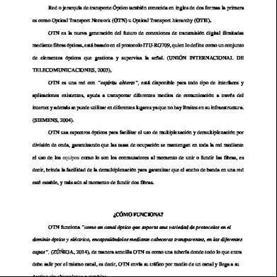
Ensayo Redes Otn z6x68
September 2021 0More Documents from "francisco morales" 4kv4g

Resumen El Socio.docx 6k382x
September 2021 0
6g3p1u
November 2019 60
6g3p1u
June 2022 0
Facturacion Electronica Siesa 4z1y3j
January 2023 0
Otn Framer Project Book 4l215z
November 2019 39