Project Report On Fm Transmitter Andreceiver 622fe
This document was ed by and they confirmed that they have the permission to share it. If you are author or own the copyright of this book, please report to us by using this report form. Report 2z6p3t
Overview 5o1f4z
& View Project Report On Fm Transmitter Andreceiver as PDF for free.
More details 6z3438
- Words: 8,502
- Pages: 35
A Project report On “Audio Transmission Using Li-Fi” Submitted in the partial fulfillment of B-Tech degree in Electronics and Communication Engineering from Rajasthan Technical University, Kota
Submitted to:
Submitted by:
Prof. Danveer Rajpal HOD (ECE.)
Mohit Bishnoi Roll No.:13EVEEC015 B.Tech.VII Sem.
VYAS INSTITUTE OF ENGINEERING AND TECHNOLOGY
Department of Electronics & Communication
VYAS INSTITUTE OF ENGINEERING & TECHNOLOGY Department of Electronics & Communication
Certificate This is to certify that Mr. Mohit Bishnoi, student of IV year B. Tech VII semester, Department of Electronics & Communication Engineering has completed the minor project on “Audio Transmission using Li-Fi” for partial fulfillment of B. Tech course for the session 2015-16 under the guidance of Mr. Saurabh Pareek.
Saurabh Pareek Assistant Professor
Danveer Rajpal HOD (ECE)
VIET(ECE),JODHPUR
2
ACKNOWLEDGEMENT I would like to express my profound gratitude towards the esteemed faculty and fellow students whose immense help and enabled me to complete this project. I would like to extend my gratefulness towards Mr. Saurabh Pareek (Asst. Prof.), who was there to guide me at each step along the way. His advice and suggestions at different points of time during the project became stepping stones for me. I extend my sincere thanks to Mr. Asharam Suthar and Mr. Dhanuprakash Purohit. It was because of their skillful teaching and instruction that I have been able to successfully complete this project. I would not have been able to do half as much as I have done without their meticulous instructions and careful help. They taught me everything that I could have learnt in the course of this project. They were always very critical of my mistakes, and because of their constructive critical nature I have been able to learn so much in the laboratory. They were always very considerate of me and gave me independence to work in the laboratory. I would also like to thank Mr. Danveer Rajpal, Head of Department of ECE, for providing the basic infrastructural facilities in the department to successfully finish this project. Lastly, I would like to acknowledge the immeasurable guidance and valuable insights I received from all the faculty which helped me through these years of pursuing Bachelors.
Name: Mohit Bishnoi Roll no.:13EVEEC015
VIET(ECE),JODHPUR
3
PREFACE
Whether you’re using wireless internet in a coffee shop, stealing it from the guy next door, or competing for bandwidth at a conference, you’ve probably gotten frustrated at the slow speeds you face when more than one device is tapped into the network. As more and more people and their many devices access wireless internet, clogged airwaves are going to make it increasingly difficult to latch onto a reliable signal. But radio waves are just one part of the spectrum that can carry our data. What if we could use other waves to surf the internet? One German physicist, DR. Harald Haas, has come up with a solution he calls “Data Through Illumination”—taking the fiber out of fiber optics by sending data through an LED light bulb that varies in intensity faster than the human eye can follow. It’s the same idea behind infrared remote controls, but far more powerful. Haas says his invention, which he calls DLight, can produce data rates faster than 10 megabits per second, which is speedier than your average broadband connection. He envisions a future where data for laptops, smartphones, and tablets is transmitted through the light in a room. And security would be a snap—if you can’t see the light, you can’t access the data. Li-Fi is a VLC, visible light communication, technology developed by a team of scientists including Dr. Gordon Povey, Prof. Harald Haas and Dr. Mostafa Afgani at the University of Edinburgh. The term Li-Fi was coined by Prof. Haas when he amazed people by streaming high definition video from a standard LED lamp, at TED Global in July 2011. Li-Fi is now part of the Visible Light Communications (VLC) PAN IEEE 802.15.7 standard. “Li-Fi is typically implemented using white LED light bulbs. These devices are normally used for illumination by applying a constant current through the LED. However, by fast and subtle variations of the current, the optical output can be made to vary at extremely high speeds. Unseen by the human eye, this variation is used to carry highspeed data,” says Dr. Povey, Product Manager of the University of Edinburgh's Li-Fi Program ‘D-Light Project’ I have made this report file on the topic Li-Fi Technology; I have tried my best to elucidate all the relevant detail to the topic to be included in the report. While in the beginning I have tried to give a general view about this topic.
VIET(ECE),JODHPUR
4
Table of Contents S.no. Title
Page no.
1 Introduction 2 Block Diagram 2.1 Description 2.1.1 Input 2.1.2 Comparator 2.1.3 Lamp Driver 2.1.4 LEDs 2.1.5 Photo Detector 2.1.6 Amplifier And Speaker 2.1.7 Output 3 Circuit Diagram &Working 3.1 Transmitter Circuit 3.2 Circuit Working 3.3 Circuit Components 3.3.1 Power Supply 3.3.2 Capacitors 3.3.3 Resistors 3.3.4 Op-Amp IC - µa 741 3.3.5 Potentiometer 3.3.6 Transistor – BC 548 3.3.7 Light Source – Led 3.4 Receiver Circuit 3.5 Circuit Working 3.6 Circuit Components 3.6.1 Photo Detector – Solar Cell 3.6.2 Speaker 3.7 The Pcb Layout 3.7.1 Pcb Design 3.7.2 Electronic Design Automation Tools 3.7.3 Pcb Design Procedures 3.7.3.1 Drawing The Circuit Schematic 3.7.3.2 Design Rule Check And Net List Creation 3.7.3.3 Creating The Pcb Artwork 3.7.3.4 Pcb Fabrication 3.7.3.5 Etching 3.7.3.6 Drilling 3.7.3.7 Soldering 3.7.4 Pcb Layout
7 9 9 10 10 10 10 10 11 11 11 11 12 13 13 14 15 16 17 18 19 20 21 21 21 22 22 22 23 23 23 23 24 24 24 25 26 28
VIET(ECE),JODHPUR
5
4 Comparison Between Li-Fi And Wi-Fi 5 Chapter 5-Result And Analysis 5.1 Advantages 5.1.1 Capacity 5.1.2 Efficiency 5.1.3 Availability 5.1.4 Security 5.1.5 No Limit For Connectivity 5.2 Limitations 5.2.1 Li-Fi Cannot Penetrate Through Walls 5.2.2 Requires Los. 5.3 Applications 5.3.1 Education Systems 5.3.2 Medical Applications 5.3.3 Cheaper Internet In Aircrafts 5.3.4 Underwater Applications 5.3.5 Disaster Management 5.3.6 Applications In Sensitive Areas 5.3.7 Traffic Management 5.3.8 Replacement For Other Technologies 6 Conclusion 7 References
28 29 30 31 31 31 31 31 31 31 31 32 32 32 32 32 33 33 34 34 34 35
VIET(ECE),JODHPUR
6
List of Figures S.no. Title
Page no.
1 Electromagnetic spectrum
8
2 Block Diagram of Li-fi
9
3 Audio Transmission Circuit
12
4 LM7805-Pinout Diagram
14
5 9V Battery
14
6 Capacitor
15
7 Resistor
15
8 Op-Amp IC – 741
17
9 Potentiometer
18
10 BC548 Transistor
19
12 LED
19
13 LED Architecture
20
14 Receiver Circuit
21
15 Solar Cell
22
16 Speaker
22
17 Li-Fi Transmitter Layout
28
18 Li-Fi Transmitter
30
19 Li-Fi Receiver
31
List of Tables S.no. Title 1. Resistor Color Codes 2. Comparison between current and future wireless Technology
Page no. 16 29
VIET(ECE),JODHPUR
7
CHAPTER 1-INTRODUCTION Over the past few years there has been a rapid growth in the utilization of the RF region of the electromagnetic spectrum. This is because of the huge growth in the number of mobile phones subscriptions in recent times. This has been causing a rapid reduction in free spectrum for future devices. Light-fidelity (Li-Fi) operates in the visible light spectrum of the electromagnetic spectrum i.e. it uses visible light as a medium of transmission rather than the traditional radio waves. Li-Fi stands for Light-Fidelity. Li-Fi is transmission of data using visible light by sending data through an LED light bulb that varies in intensity faster than the human eye can follow. If the LED is on, the photo detector s a binary one; otherwise it’s a binary zero. The idea of Li-Fi was introduced by a German physicist, Harald Hass, which he also referred to as “Data through Illumination”. The term Li-Fi was first used by Haas in his TED Global talk on Visible Light Communication. According to Hass, the light, which he referred to as “DLight‟, can be used to produce data rates higher than 1 Giga bits per second which is much faster than our average broadband connection. The high speed achievement of Li-Fi can be explained using frequency spectrum of Electromagnetic Radiations. From the electromagnetic spectrum we can see that the frequency Band of the visible light is in between 430THz to 770THz and that of Radio Frequency Band is in between 1Hz to 3THz, Hence the Frequency Bandwidth of the visible light is about 400 Times greater than the Radio Frequency Bandwidth. So more Number of bits can be transferred through this Bandwidth than in the radio frequency bandwidth. Hence Data rate will be higher in the Li-Fi and higher speed can be achieved. Using Li-Fi we can transmit any data that can be transferred using conventional Wi-Fi network. That can be Images, Audio, Video, Internet connectivity, etc. but the advantages over the Wi-Fi Network Are High speed, Increased Security, More Number of Connected Devices, and Less cost. In coming years’ number of devices that Li-Fi will hit the Market. It is estimated that the compound annual growth of Li-Fi market will be 82% from 2015 to 2018 and to be worth over $6 billion per year by 2018.
VIET(ECE),JODHPUR
8
Figure.1.1Electromagnetic Spectrum This Mini Project discusses the implementation of the most basic Li-Fi based system to transmit Sound signal from one device to another through visible light. The purpose is to demonstrate only the working of the simplest model of Li-Fi with no major consideration about the data transfer speed. This model will demonstrate how the notion of one-way communication via visible light works, in which Light emitting diodes (LEDs) are employed as the light sources or Transmitter antennas. The model will transmit digital signal via direct modulation of the light. The emitted light will be detected by an optical receiver. In addition to the demonstration purpose, the model enables investigation into the features of the visible light and LEDs incorporated in the communication model.
CHAPTER 2-BLOCK DIAGRAM
VIET(ECE),JODHPUR
9
Figure.2.1 Block Diagram
2.1 DESCRIPTION The basic block diagram consists of Input from the Source Comparator. Lamp Driver. LEDs. Photo Detector. Amplifier and Speaker. Output at the Destination 2.1.1 INPUT Input consists of analog signal, which is usually taken from the Audio output of the Mobile Phone, Laptop or any other Musical Instruments. The signal will be at low voltage level which is not enough to drive an LED, so in order to drive the LEDs we have to amplify the signal using amplifiers. 2.1.2 COMPARATOR The input signal from an audio device will be at low voltage level, so in order to modulate the signal using visible light, we have to convert the signal in to a Pulse wave format (signal representing 0 & 1). to accomplish this task, we use an Op-Amp Comparator which uses µA 741 Op-Amp IC. The comparator compares the input signal with a reference voltage and produces an output which will be in Pulse wave form. The pulse wave so formed is amplified and modulated at the Lamp Driver. 2.1.3 LAMP DRIVER The pulse wave from the comparator has to be amplified to drive the LEDs. And Modulation of the input signal and Carrier Light signal is also taking place at the Lamp driver using a
VIET(ECE),JODHPUR
10
Transistor called BC 548, which is general purpose Silicon Transistor uses as Amplification transistor as well as Modulation transistor. The amplified and modulated pulse signal is used to drive the LEDs. These LEDs transmit the modulated signals to the receiver. 2.1.4 LEDs In Li-Fi Transmission, the most important requirement of light source is its ability to turn ON and OFF Repeatedly in very short intervals (in ns range). So we use LEDs which have very low switching time. These LEDs turn ON and OFF in Nano second based on the Pulse signal. Since the switching taking at a faster rate, it cannot be detected by Human eye. So it will appear as illuminating even though they are blinking. Thus modulated signal is transmitted to receiver via Visible Light. 2.1.5 PHOTO DETECTOR The transmitted signal from the LEDs has to be detected, demodulated and acknowledged. So in order to detect the message signal from the blinking LED light, we use a photo cell or a Solar Cell (which comprises large no of photo cells connected in series). The solar cell detects only the variation of the light, since the blinking can be easily detected and output of the solar cell will be the message signal in the analog form. So using solar we could detect and demodulate the message signal transmitted.
2.1.6 AMPLIFIER AND SPEAKER The demodulated signal will be at low voltage range. So it is Amplified to the arbitrary voltage level using an amplifier. This amplifier will be same type of amplifier which we used in transmitter side. This is due to the fact that if any phase errors occurred, it will be cleared at this stage. The speaker will convert the electrical signal to the audible form using electro magnets present in the speaker. 2.1.7 OUTPUT The demodulated audible signal is transmitted from speaker to its final destination. So that the audience can listen to the message that has been transmitted from the source
VIET(ECE),JODHPUR
11
CHAPTER 3-CIRCUIT DIAGRAM &WORKING 3.1 TRANSMITTER CIRCUIT
Figure.3.1.1 Li-Fi Audio Transmitter Circuit 3.2 CIRCUIT WORKING The above figure depicts the transmitter circuit of the Li-Fi circuit. We know that carrier waves can take signals along destinations, so this is simple concept when we put photons with speed of light by source to destination it can also carry signals of low frequency to destination. so we build a circuit which can modulate light with low frequency signals. Take input from an audio device, the input will be very low audio signals of 20Hz to 20KHz. These signals paces through C1 (100nf) where DC (Direct Current) components are filtered and removed. Through R3 100kΩ which is a current limit for comparator µA741 (Op-Amp) to protect it from the high current which cause destruction of the Op-Amp. Through R1 100kΩ and R4 100kΩ, voltage at the inverting terminal of the Op-Amp limit to 5v/2 = 2.5v. Input signal at pin 3 of op-amp and compare with pin 2 of Op-Amp and output will be
VIET(ECE),JODHPUR
12
present at the Pin No 6 of the Op-Amp IC. 470kΩ pot or gain controller to control volume at output of the Op-Amp If there is no input is fed to the Comparator, a Positive DC wave will present at pin 6 of Op-Amp, which make transistor Q1 keep alive and LED starts to glow Continuously. The Capacitors C3, C4 (Both are 470µF) are filters to reduce AC components spike in circuit. Whenever signals interrupt through pin 3 of op-amp (input from Audio device). The Comparator compares the input signal with the Reference Voltage and produce a Pulse wave output at the Pin 6. The width of the pulse wave is controlled by the Input Signal Frequency. The Pulse signal is equivalent to the ON/OFF Signal which control the intensity of the Light Source aka LED (D1). The Pulse wave is further Amplified and Modulated using Transistor BC548 (T1), which is an Amplifier Modulator having high current gain. The transistor will act as a Lamp Driver and drives the LED. LED emits light according to the pulse wave form and make VLC (Visible light communication) alive. Since the blinking of the LED is controlled by the input signal, it will take place in Nano Seconds (ns) it cannot detect by Human eyes. 3.3 CIRCUIT COMPONENTS The Basic Components of the Transmitter Circuits are Power Supply (9V Supply) Capacitors Resistors Op-Amp IC - µA 741 Potentiometer (Audio / Controller) Transistor – BC 548 Light Source – LEDs
VIET(ECE),JODHPUR
13
3.3.1 POWER SUPPLY The power supply is the most indispensable part of any project. IC Regulators are versatile and relatively inexpensive and are available with features such as current/voltage boosting,
internal short circuit current limiting, thermal shutdown and floating operation for high voltage applications. The regulated circuit is used to maintain constant output level. The regulator IC here used is LM 7805. It provides regulated 5V to the Circuit. Its maximum input voltage is 35V and minimum voltage is 8V. Output is Constant 5V. The Pin out diagram of LM 7805 IC is given below LM 7805 Have several Features; they are listed below. Figure.3.3.1.1 LM7805 – Regulator IC Features of LM 7805 Regulator are
Output current is up to 1.5A Output Voltage of 5,5.2,6,8,8.5,9,12,15,18,24V Thermal overload Protection Short circuit Protection Output Transition SOA Protection Maximum input Voltage = 35V We can also use 5V DC Cell for the power supply of the circuit.
VIET(ECE),JODHPUR
14
Figure.3.3.1.2 9V Battery
3.3.2 CAPACITORS
Figure.3.3.2.1 Capacitor A capacitor is a two-terminal, electrical component. Along with resistors and inductors, they are one of the most fundamental ive components we use. What makes capacitors special is their ability to store energy; they’re like a fully charged electric battery. Caps, as we usually refer to them, have all sorts of critical applications in circuits. Common applications include local energy storage. Capacitance is its Unit. Not all capacitors are created equal. Each capacitor is built to have a specific amount of capacitance. The capacitance of a capacitor tells you how much charge it can store; more capacitance means more capacity to store charge. The standard unit of capacitance is called the farad, which is abbreviated F. It turns out that a farad is a lot of capacitance, even 0.001F (1 milli farad – 1mF) is a big capacitor. Usually we’ll see capacitors rated in the Pico- (10 -12) to microfarad (10-6) range. 3.3.3 RESISTORS
Figure.3.3.3.1 Resistors Resistors are the most commonly used component in electronics and their purpose is to create specified values of current and voltage in a circuit. The unit for measuring resistance is the OHM. (The Greek letter Ω - called Omega). Higher resistance values are
VIET(ECE),JODHPUR
15
represented by "k" (kilo-ohms) and M (Mega ohms). For example, 120 000 Ω is represented as 120k, while 1200000 Ω is represented as 1MΩ. The dot is generally omitted as it can easily be lost in the printing process. In some circuit diagrams, a value such as 8 or 120 represents a resistance in ohms. Another common practice is to use the letter E for resistance in ohms. The letter R can also be Resistor Markings. Resistance value is marked on the resistor body. Most resistors have 4 bands. The first two bands provide the numbers for the resistance and the third band provides the number of zeros. The fourth band indicates the tolerance. Tolerance values of 5%, 2%, and 1% are used. The following table shows the Color Code used to identify resistor values. COLOR
DIGIT
MULTIPLIER TOLERANCE
Silver
x 0.01 W
±10%
Gold
x 0.1 W
±5%
TC
Black
0
x1W
Brown
1
x 10 W
±1%
±100*10-6/K
Red
2
x 100 W
±2%
±50*10-6/K
Orange
3
x 1 kW
±15*10-6/K
Yellow
4
x 10 kW
±25*10-6/K
Green
5
x 100 kW
±0.5%
Blue
6
x 1 MW
±0.25%
±10*10-6/K
Violet
7
x 10 MW
±0.1%
±5*10-6/K
Grey
8
x 100 MW
White
9
x 1 GW
±1*10-6/K
Table 3.3.3.2 Resistor Color Codes
VIET(ECE),JODHPUR
16
3.3.4 Op-Amp IC - µA 741
Figure.3.3.4.1 Op-Amp IC - µA 741 An operational amplifier (op-amp) is a DC-coupled high-gain electronic voltage amplifier with a differential input and, usually, a single-ended output. In this configuration, an op-amp produces an output potential (relative to circuit ground) that is typically hundreds of thousands of times larger than the potential difference between its input terminals. Operational amplifiers had their origins in analog computers, where they were used to do mathematical operations in many linear, non-linear and frequency-dependent circuits. The popularity of the op-amp as a building block in analog circuits is due to its versatility. Due to negative , the characteristics of an op-amp circuit, its gain, input and output impedance, bandwidth etc. are determined by external components and have little dependence on temperature coefficients or manufacturing variations in the op-amp itself. Op-amps are among the most widely used electronic devices today, being used in a vast array of consumer, industrial, and scientific devices. Many standard IC op-amps cost only a few cents in moderate production volume; however, some integrated or hybrid operational amplifiers with special performance specifications may cost over $100 US in small quantities. Op-amps may be packaged as components, or used as elements of more complex integrated circuits. The op-amp is one type of differential amplifier. Other types of differential amplifier include the fully differential amplifier (similar to the op-amp, but with two outputs), the instrumentation amplifier (usually built from three op-amps), the isolation amplifier (similar to the instrumentation amplifier, but with tolerance to common-mode voltages that would destroy an ordinary op-amp), and negative amplifier (usually built from one or more op-amps and a resistive network).
VIET(ECE),JODHPUR
17
Features of Op-Amp IC Short-Circuit Protection Offset-Voltage Null Capability. Large Common-Mode and Differential Voltage Ranges. No Frequency Compensation Required and Latch up A-741is general Purpose operational amplifier. The device exhibits high stability. It can be configured in inverting and Non-Inverting Mode It can be used to implement comparators, Astable, Monostable Multvibrators. Amplifiers, etc. 3.3.5 POTENTIOMETER
Figure.3.3.5.1 Potentiometer A potentiometer, informally a pot, is a three-terminal resistor with a sliding or rotating that forms an adjustable voltage divider. If only two terminals are used, one end and the wiper, it acts as a variable resistor or rheostat. The measuring instrument called a potentiometer is essentially a voltage divider used for measuring electric potential (voltage); the component is an implementation of the same principle, hence its name. Potentiometers are commonly used to control electrical devices such as volume controls on audio equipment. Potentiometers operated by a mechanism can be used as position transducers, for example, in a joystick. Potentiometers are rarely used to directly control significant power (more than a watt), since the power dissipated in the potentiometer would be comparable to the power in the controlled load.
VIET(ECE),JODHPUR
18
3.3.6 TRANSISTOR – BC 548
Figure.3.3.6.1 BC 548 Transistor It is general purpose silicon, NPN, bipolar junction transistor. It is used for amplification and switching purposes. The current gain may vary between 110 and 800. The maximum DC current gain is 800.Its equivalent transistors are 2N3904 and 2SC1815. These equivalent transistors however have different lead assignments. The variants of BC548 are 548A, 548B and 548C which vary in range of current gain and other characteristics. The transistor terminals require a fixed DC voltage to operate in the desired region of its characteristic curves. This is known as the biasing. For amplification applications, the transistor is biased such that it is partly on for all input conditions. The input signal at base is amplified and taken at the emitter. BC 548 is used in common emitter configuration for amplifiers. The voltage divider is the commonly used biasing mode. For switching applications, transistor is biased so that it remains fully on if there is a signal at its base. In the absence of base signal, it gets completely off. 3.3.7 LIGHT SOURCE – LED
Figure.3.3.7.1 LED
VIET(ECE),JODHPUR
19
The most important requirement that a light source has to meet in order to serve communication purposes is the ability to be switched on and off repeatedly in very short intervals. By utilizing the advantage of fast switching characteristics of LED ‟s compared with the conventional lightning, the LED illumination is used as a communication source. Since the illumination exists everywhere, it is expected that the LED illumination device will act as a lighting device and a communication transmitter simultaneously everywhere in a near future. Typically, red, green, and blue LEDs emit a band of spectrum, depending on the material system. The white LED draws much attention for the illumination devices. Comparing the LED illumination with the conventional illumination such as fluorescent lamps and incandescent bulbs, the LED illumination has many advantages such as high efficiency, environment-friendly manufacturing, design flexibility, long lifetime, and better spectrum performance. LEDs emit light when energy levels change in the semiconductor diode. This shift in energy generates photons, some of which are emitted as light. The specific wavelength of the light depends on the difference in energy levels as well as the type of semiconductor material used to form the LED chip. Solid-state design allows LEDs to withstand shock, vibration, frequent switching (electrical on and off shock) and environmental (mechanical shocks) extremes without compromising their famous long life typically 100,000 hours or more. The basic LED consists of a semiconductor diode chip mounted in the reflector cup of a lead frame that is connected to electrical (wire bond) wires, and then encased in a solid epoxy lens. The architecture of LED is shown in Figure.
Figure.3.3.7.2 LED Architecture
VIET(ECE),JODHPUR
20
3.4 RECEIVER CIRCUIT
Figure.3.4.1 Receiver Circuit 3.5 CIRCUIT WORKING The Solar cell is used to detect the Light from the Transmitting LEDs. And it produces an Analog output corresponding to the input signal. The frequency of the analog will be same as that of input signal, since the flickering of LED is controlled by the input signal and solar cell detects only the fluctuation in the LED signal and produces the output. The output is then amplified using BC 548. It also helps in removing any phase changes occurs in the transmitted signal. The Amplified signal is fed to the speaker. The speaker converts the analog signal to the Audible Sound signal using the electromagnet present in the Speaker. 3.6 CIRCUIT COMPONENTS The basic Components of the Receiver Circuits are Photo Detector – Solar cell Transistor - BC 548 Speaker
VIET(ECE),JODHPUR
21
3.6.1 PHOTO DETECTOR – SOLAR CELL
Figure.3.6.1.1 Solar Cell A Solar cell is an electrical device that converts the energy of Light Directly to electric signal or analog signal by the photovoltaic effect, which is a chemical physical phenomenon. When photons are strikes on its walls electron flow occurs which will store as electrical energy. It has slower Time response as their area increases. Solar cells are formed connecting large Number of Photo Detectors connected in series. It works in the Reverse Biased Mode. Usually the Efficiency of solar cell is Low. Even though it regarded as Green Technology.
3.6.2 SPEAKER
Figure.3.6.2.1 Speaker
VIET(ECE),JODHPUR
22
In this project we use Speaker which has in-built Amplifier, which Amplifies the Analog signal received from the output of the Solar cell. It also helps to remove any phase errors that may occurred during the Transmitting or Processing of the input signal. The main Function of a speaker is to convert Electrical or Analog Signals in to the Audible form to reach the Receptor. It converts the sound signal with the help of Electromagnets Present in the Speaker. Hence the Receptor Receive the input that has been transmitted from the Transmitter. 3.7 THE PCB LAYOUT 3.7.1 PCB DESIGN Design of printed circuit board (PCB) can be considered as the last step in electronic circuit design as well as the first step in production. It plays important role in the performance and reliability of electronic circuits, the productivity of the PCB’s its assembling, and its service ability depends on design. All these factors get reflected in a piece of electronic equipment. It is clear that task of PCB design is not very simple or always straight forward. The schematic is follower by layout generation. Layout design is the stage where engineering capacity combined with creativity is the governing inputs.
3.7.2 ELECTRONIC DESIGN AUTOMATION TOOLS Most product testing is being done is done with the help of computer programs. The term Electronic Design Automation (EDA) is being used to describe the use of these tools. With the help of advanced powerful computing systems and interactive software tools and development of electronic circuits has undergone automation. Thus the software and hardware tools, which enables this automation includes PCB deg, IC design, circuit simulation etc. These tools help us in such a way that we can draw the circuit; test the functioning of the circuit in response to test inputs in simulation software. After successfully simulation we can get the PCB art work done by replacing the routing software. The design automation tool used here is EXPRESS PCB.
VIET(ECE),JODHPUR
23
3.7.3 PCB DESIGN PROCEDURES The PCB deg procedure consists of following steps: 3.7.3.1 DRAWING THE CIRCUIT SCHEMATIC
Drawing of circuit is done through EXPRESS PCB. It includes many libraries with thousands of component symbols. We can select the required symbol from the library and place it in the schematic page. After placing the component symbols, we can complete the interconnection using wire or bus control. The next step is to assign part reference. Each component has to be assigned footprint or PCB pattern name. The footprint gives the actual size physical representation of components on the PCB artwork. The component symbol and foot symbol should correspond in all respects.
3.7.3.2 DESIGN RULE CHECK AND NET LIST CREATION
After the circuit schematic is completed with all required information such as part reference and footprints, the design rule check can be used for checking errors in the design. It will check for duplicate symbols, overlapped lines and dangling lines. After the schematic design file es the DRC check, it is processed by a program called an electric rule checker (ERC) that checks for writing errors. The final operation to be done before starting PCB artwork is the net list creation. A net list creation of the components and interconnection along with other information such as foot prints, track width etc. A net list software or tool can take the circuit schematic as input and generate net list. The net list can be used as an information source for the remaining stages. 3.7.3.3 CREATING THE PCB ARTWORK
In automatic design, the net list obtained from the previous stage is used for getting the required foot print and interconnections. The software used for the PCB artwork design in the EXPRESS PCB. 3.7.3.4 PCB FABRICATION
You need to generate a positive (copper black) UV translucent art work film. You will never get a good board without good art work, so it is important to get the best possible quality at this stage. The most important thing is to get a clear sharp image with a very solid opaque black. Art work is done using EXPRESS PCB software. It is absolutely essential that
VIET(ECE),JODHPUR
24
your PCB software prints holes in the middle of pads, which will act as center marks when drilling. It is virtually impossible to accurately hand-drill boards without these holes. If you are looking to buy PCB software at any cost level and want to do hand-prototyping of boards before production, check that this facility is available when defining pad and line shapes, the minimum size recommended (through-linking holes) for reliable result is 50 mil, assuming 0.8mm drill size; 1 mil= (1/1000) th of an inch. You can go smaller drill sizes, but through linking will be harder. 65mil round or square pads for normal components. ICs, with 0.8 mm hole, will allow a 12.5mil, down to 10mil if you really need to. Center-to-center spacing of 12.5 mil tracks should be 25 mil-slightly less may be possible if your printer can manage it. Take care to preserve the correct diagonal track-track spacing on mitered corners; grid is 25 mil and track width 12.5mil. The art work must be printed such that the printed side is in with PCB surface when exposing, to avoid blurred edges. In practice, this means that if you design the board as seen from the component side, the bottom (solder side) layer should be printed the “correct” way round, and top side of the doublesided board must be printed mirrored.
3.7.3.5 ETCHING
Ferric chloride etchant is a messy stuff, but easily available and cheaper than most alternatives. It attacks any metal including stainless steel. So when setting up a PCB etching area, use a plastic or ceramic sink, with plastic fitting and screws wherever possible, and seal any metal screws with silicon. Copper water pipes may be splashed or dripped-on, so sleeve or cover them in plastic; heat-shrink sleeve is great if you are installing new pipes. Fume extraction is not normally required, although a cover over the tank or tray when not in use is a good idea. You should always use the hex hydrate type of ferric chloride, which should be dissolved in warm water until saturation. Adding a teaspoon of table salt helps to make the etchant clearer for easier inspection. Avoid anhydrous ferric chloride. It creates a lot of heat when dissolved. So always add the powder very slowly to water; do not add water to the powder, and use gloves and safety glasses. The solution made from anhydrous ferric chloride doesn’t etch at all, so you need to add a small amount of hydrochloric acid and leave it for a day or two. Always take extreme care to avoid splashing when dissolving either type of ferric chloride, acid tends to clump together and you often get big chunks coming out of the container and splashing into the solution. It can damage eyes and permanently stain clothing. If you are making PCBs in a professional environment where time is money you should get a heated bubble-etch tank. With fresh hot ferric chloride, the PCB will etch in well under 5 minutes. Fast etching produces better edge-quality and consistent line widths. If you aren’t
VIET(ECE),JODHPUR
25
using a bubble tank, you need to agitate frequently to ensure even etching. Warm the etchant by putting the etching tray inside a larger tray filled with boiling water. 3.7.3.6 DRILLING
If you have fiber glass (FR4) board, you must use tungsten carbide drill bits. Fiberglass eats normal high-speed steel (HSS) bits very rapidly, although HSS drills are alright for older larger sizes (> 2mm). Carbide drill bits are available as straight-shank or thick-shank. In straight shank, the hole bit is the diameter of the hole, and in thick shank, a standard size (typically about 3.5 mm) shank tapers down to the hole size. The straight-shank drills are usually preferred because they break less easily and are usually cheaper. The longer thin section provides more flexibility. Small drills for PCB use usually come with either a set of collets of various sizes or a three-jaw chuck. Sometimes the 3-jaw chuck is an optional extra and is worth getting for the time it saves on changing collets. For accuracy, however, 3-jaw chucks are not brilliant, and small drill sizes below 1 mm quickly formed grooves in the jaws, preventing good grip. Below 1 mm, you should use collets, and buy a few extra of the smallest ones; keeping one collect per drill size as using a larger drill in a collet will open it out and it no longer grips smaller drills well. You need a good strong light on the board when drilling, to ensure accuracy. A dichroic halogen lamp, under run at 9V to reduce brightness, can be mounted on a microphone gooseneck for easy positioning. It can be useful to raise the working surface above 15 cm above the normal desk height for more comfortable viewing. Dust extraction is nice, but not essential and occasional blow does the trick! A foot-pedal control to switch the drill “off” and “on” is very convenient, especially when frequently changing bits. Avoid hole sizes less than 0.8 mm unless you really need them. When making two identical boards, drill them both together to save time. To do this, carefully drill a 0.8 mm whole in the pad near each corner of each of the two boards, getting the center as accurately as possible. For larger boards, drill a hole near the center of each side as well. Lay the boards on the top of each other and insert a 0.8 mm track pin in two opposite corners, using the pins as pegs to line the PCBs up. Squeeze or hammer the pins into boards, and then into the remaining holes. The two PCBs are now “nailed” together accurately and can be drilled together. 3.7.3.7 SOLDERING
Soldering is the ing together of two metals to give physical bonding and good electrical conductivity. It is used primarily in electrical and electronic circuitry. Solder is a combination of metals, which are solid at normal room temperatures and become liquid between 180 and 200 degrees Celsius. Solder bonds well to various metals, and extremely well to copper. Soldering is a necessary skill you need to learn to successfully build
VIET(ECE),JODHPUR
26
electronics circuits. To solder you need a soldering iron. A modern basic electrical soldering iron consists of a heating element, a soldering bit (often called a tip), a handle and a power cord. The heating element can be either a resistance wire wound around a ceramic tube, or a thick film resistance element printed on to a ceramic base. The element is then insulated and placed into a metal tube for strength and protection. This is then thermally insulated from the handle. The heating element of soldering iron usually reaches temperatures of around 370 to 400 degree Celsius (higher than need to melt the solder). The strength or power of a soldering iron is usually expressed in watts. Irons generally used in electronics are typically in the range of 12 to 25 watts. Higher powered iron will not run hotter. Most irons are available in a variety of voltages; 12V, 24V, 115V and 230V are most popular. Today most laboratories and repair shops use soldering irons, which operate at 24V. You should always use this low voltage where possible, as it is much safer. For advanced soldering work, you will need a soldering iron with temperature control. In this type of soldering irons, the temperature may be usually set between 200 and 450 degrees Celsius. Many temperature control soldering iron designed for electronics have a power rating of around 40 to 50 watt. They will heat fast and give enough power for operation, but are mechanically small. You will occasionally see gas-powered soldering irons which use butane rather than the main electrical supply to operate. They have a catalytic element which once warmed up, continues to glow hot when gas es over them. Gas powered soldering irons are designed for occasional “on the spot” used for quick repairs, rather than for main stream construction or for assembly work. Currently, the best commonly available, workable, and safe solder alloy is 63/37. That is, 63% lead, 37% tin. It is also known as eutectic solder. Its most desirable characteristic is that it solids (“pasty”) state, and its liquid state occur at the same temperature -361 degree Fahrenheit. The combination of 63% lead and 37% tin melts at the lowest possible temperature. Nowadays there is tendency to move to use lead free solders, but it will take years until they catch on normal soldering work. Lead free solders are nowadays available, but they are generally more expensive or harder to work on than traditional solders that they have lead in them. The metals involved are not the only things to consider in a solder. Flux is vital to a good solder t. Flux is an aggressive chemical that removes oxide and impurities from the parts to be soldered. The chemical reactions at the point(s) of connection must take place for the metal to fuse. RMA type flux (Rosin Mildly Active) is the least corrosive of the readily available materials, and provides an adequate oxide. In electronics, a 60/40 fixed core solder is used. This consists of 60% lead and 40% tin, with flux cores added to the length of solder.
VIET(ECE),JODHPUR
27
There are certain safety measures which you should keep in mind when soldering. The tin material used in soldering contains dangerous substances like lead (40-60% of typical soldering tins are lead and lead is poisonous). Also the various fumes from the soldering flux can be dangerous. While it is true that lead does not vaporize at the temperature at which soldering is typically done. When soldering, keep the room well ventilated and use a small fan or fume trap. A proper fume trap of a fan will keep the most pollution away from your face. Professional electronic workshops use expensive fume extraction systems to protect their workers. Those fume extraction devices have a special filter which filters out the dangerous fumes. If you can connect a duct to the output from the trap to the outside, that would be great. Always wash hands prior to smoking, eating, drinking or going to the bathroom. When you handle soldering tin, your hands will pick up lead, which needs to be washed out from it before it gets to your body. Do not eat, drink or smoke while working with soldering iron. Do not place cups, glasses or a plate of food near your working area.
3.7.4 PCB LAYOUT
Figure.3.7.4.1 Li-Fi Transmitter Layout
VIET(ECE),JODHPUR
28
CHAPTER 4 4.1 COMPARISON BETWEEN Li-Fi and Wi-Fi Li-Fi is a term of one used to describe visible light communication technology applied to high speed wireless communication. It acquired this name due to the similarity to Wi-Fi, only using light instead of radio. Wi-Fi is great for general wireless coverage within buildings, and Li-Fi is ideal for high density wireless data coverage in confined area and for relieving radio interference issues, so the two technologies can be considered complimentary.
Technology
Speed
Data Density
Wireless (Current) Wi-Fi – IEEE 150 Mbps 802.11n
*
Bluetooth
3 Mbps
*
IrDA
4 Mbps
***
Wireless (Future) WiGig
2 Gbps
**
Giga-IR
1 Gbps
***
Li-Fi
>1Gbps
****
Table.4.1 Comparison between current and future wireless Technology The table also contains the current wireless technologies that can be used for transferring data between devices today, i.e. Wi-Fi, Bluetooth and IrDA. Only Wi-Fi currently offers very high data rates. The IEEE 802.11.n in most implementations provides up to 150Mbit/s (in theory the standard can go to 600Mbit/s) although in practice you receive considerably less than this. Note that one out of three of these is an optical technology.
CHAPTER 5-RESULT AND ANALYSIS In our project we Designed and implemented a wireless communication device which Transmit Audio Message wirelessly known as LIGHT FIDELITY (Li-Fi). The project contains two sections 1 – Transmitter Section and 2 – Receiver Section. The transmitter
VIET(ECE),JODHPUR
29
section Modulate the incoming message audio signal and transmit towards the receiver in the form Visible Light using LEDs. The receiver section interprets the incoming light which is detected using a solar and converts to the audible sound signal with the help of Speaker.
Figure.5.1 Li-Fi Transmitter
Figure.5.2 Li-Fi Receiver
VIET(ECE),JODHPUR
30
5.1 ADVANTAGES Li-Fi technology is based on LEDs or other light source for the transfer of data. The transfer of the data can be with the help of all kinds of light, no matter the part of the spectrum that they belong. That is, the light can belong to the invisible, ultraviolet or the visible part of the spectrum. Also, the speed of the communication is more than sufficient for ing movies, games, music and all in very less time. Also, Li-Fi removes the limitations that have been put on the by the Wi-Fi. 5.1.1 CAPACITY Light has 400 times wider bandwidth than radio waves. Also, light sources are already installed. So, Li-Fi has got better capacity and also the infrastructures are already available. 5.1.2 EFFICIENCY Data transmission using Li-Fi is very cheap. LED lights consume less energy and are highly efficient and long lasting. 5.1.3 AVAILABILITY Availability is not an issue as light sources are presents everywhere. There are billions of light bulbs worldwide, they just need to be replaced with LEDs for proper transmission of data. 5.1.4 SECURITY Light waves do not penetrate through walls. So, they can’t be intercepted and misused. 5.1.5 NO LIMIT FOR CONNECTIVITY The High speed capability of Li-Fi enables large number s can be connected, since speed will not be throttled or slowed down. 5.2 LIMITATIONS The major Limitations of this technology are
VIET(ECE),JODHPUR
31
5.2.1 Li-Fi CANNOT PENETRATE THROUGH WALLS The artificial light cannot penetrate into walls and other opaque materials which radio waves can do. So a Li-Fi enabled end device (through its inbuilt photo-receiver) will never be as fast and handy as a Wi-Fi enabled device if any obstacle is present between Transmitter and Receiver.
5.2.2 REQUIRES LoS. To function Li-Fi with full efficiency, It Requires Line of Sight. That is the Transmitter Antenna and Receiver Antenna should be in a line (Face to Face). Still, Li-Fi could emerge as a boon to the rapidly depleting bandwidth of radio waves. And it will certainly be the first choice for accessing internet in a confined room at cheaper cost. 5.3 APPLICATIONS There are numerous applications of this technology, from public internet access through street lamps to auto-piloted cars that communicate through their headlights. Applications of Li-Fi can extend in areas where the Wi-Fi technology lacks its presence like medical technology, power plants and various other areas. Since Li-Fi uses just the light, it can be used safely in aircrafts and hospitals where Wi-Fi is banned because they are prone to interfere with the radio waves. All the street lamps can be transferred to Li-Fi lamps to transfer data. As a result of it, it will be possible to access internet at any public place and street. Some of the future applications of Li-Fi are as follows 5.3.1 EDUCATION SYSTEMS Li-Fi is the latest technology that can provide fastest speed internet access. So, it can replace Wi-Fi at educational institutions and at companies so that all the people can make use of Li-Fi with the same speed intended in a particular area. 5.3.2 MEDICAL APPLICATIONS Operation theatres (OTs) do not allow Wi-Fi due to radiation concerns. Usage of WiFi at hospitals interferes with the Mobile and PC which blocks the signals for monitoring equipment. So, it may be hazardous to the patient's health. To overcome this and to make OT tech savvy Li-Fi can be used to accessing internet and to control medical equipment. This can even be beneficial for robotic surgeries and other automated procedures.
VIET(ECE),JODHPUR
32
5.3.3 CHEAPER INTERNET IN AIRCRAFTS The engers travelling in aircrafts get access to low speed internet at a very high rate. Also Wi-Fi is not used because it may interfere with the navigational systems of the pilots. In aircrafts Li-Fi can be used for data transmission. Li-Fi can easily provide high speed internet via every light source such as overhead reading bulb, etc. present inside the airplane. 5.3.4 UNDERWATER APPLICATIONS Underwater ROVs (Remotely Operated Vehicles) operate from large cables that supply their power and allow them to receive signals from their pilots above. But the tether used in ROVs is not long enough to allow them to explore larger areas. If their wires were replaced with light say from a submerged, high-powered lamp then they would be much freer to explore. They could also use their headlamps to communicate with each other, processing data autonomously and sending their findings periodically back to the surface. Li-Fi can even work underwater where Wi-Fi fails completely, thereby throwing open endless opportunities for military operations. 5.3.5 DISASTER MANAGEMENT Li-Fi can be used as a powerful means of communication in times of disaster such as earthquake or hurricanes. The average people may not know the protocols during such disasters. Subway stations and tunnels, common dead zones for most emergency communications, pose no obstruction for Li-Fi. Also, for normal periods, Li-Fi bulbs could provide cheap high-speed Web access to every street corner. 5.3.6 APPLICATIONS IN SENSITIVE AREAS Power plants need fast, inter-connected data systems so that demand, grid integrity and core temperature (in case of nuclear power plants) can be monitored. Wi-Fi and many other radiation types are bad for sensitive areas surrounding the power plants. Li-Fi could offer safe, abundant connectivity for all areas of these sensitive locations. This can save money as compared to the currently implemented solutions. Also, the pressure on a power plants own reserves could be lessened. Li-Fi can also be used in petroleum or chemical plants where other transmission or frequencies could be hazardous. 5.3.7 TRAFFIC MANAGEMENT In traffic signals Li-Fi can be used which will communicate with the LED lights of the cars which can help in managing the traffic in a better manner and the accident numbers can be decreased. Also, LED car lights can alert drivers when other vehicles are too close.
VIET(ECE),JODHPUR
33
5.3.8 REPLACEMENT FOR OTHER TECHNOLOGIES Li-Fi doesn’t work using radio waves. So, it can be easily used in the places where Bluetooth, infrared, Wi-Fi, etc. are banned.
CHAPTER 6-CONCLUSION The possibilities are numerous and can be explored further. If his technology can be put into practical use, every bulb can be used something like a Wi-Fi hotspot to transmit wireless data and we will proceed toward the cleaner, greener, safer and brighter future. The concept of Li-Fi is currently attracting a great deal of interest, not least because it may offer a genuine and very efficient alternative to radio-based wireless. As a growing number of people and their many devices access wireless internet, the airwaves are becoming increasingly clogged, making it more and more difficult to get a reliable, high-speed signal. This may solve issues such as the shortage of radio-frequency bandwidth and also allow internet where traditional radio based wireless isn’t allowed such as aircraft or hospitals. The main shortcoming however is that it only work in direct line of sight. 6.1 FUTURE SCOPE By using Li-Fi we can have Energy saving Parallelism. With growing number of people and their many devices access wireless internet, on one-way data transfer at high speed and at cheap cost. In future we can have LED array beside a motorway helping to light the road, displaying the latest traffic updates and transmitting internet information to wirelessly to engers Laptops, Notebooks and Smart phones. This is the kind of extra ordinary, energy saving parallelism that is believed to deliver by this pioneering technology.
VIET(ECE),JODHPUR
34
REFERENCES
http://en.wikipedia.org/wiki/Li-Fi www.YouTube.com – TED Talk by Harald Hass on Li-Fi “Li-Fi (Light Fidelity)-The future technology in Wireless communication?” by Jyoti
Rani. “Journal from International Journal of Applied Engineering Research” (IJAER); ISSN 0973- 4562 Vol.7 No.11 (2012) www.lificonsortium.org/ Priyanka Dixit and Kunal Lala – Li-Fi the Latest Technology in Wireless; ISBN
978817515738 seminarprojects.com/s/seminar-report-on-lifi http://en.wikipedia.org/wiki/Li-Fi http://teleinfobd.blogspot.in/2012/01/what-is-lifi.html technopits.blogspot.comtechnology.cgap.org/2012/01/11/a-lifi-world/ www.lificonsortium.org/ the-gadgeteer.com/2011/08/29/li-fi-internet-at-thespeed-of-light/ en.wikipedia.org/wiki/Li-Fi www.macmillandictionary.com/buzzword/entries/Li- Fi.html dvice.com/archives/2012/08/lifi-ten-ways-i.php Will Li-Fi be the new Wi-Fi? New Scientist, by Jamie Condliffe, dated 28 July 2011 http://www.digplanet.com/wiki/Li-Fi ” Visible-light communication: Tripping the light fantastic: A fast and cheap optical version of Wi-Fi is coming”, Economist, dated 28Jan 2012
VIET(ECE),JODHPUR
35
Related Documents c2h70

Project Report On Fm Transmitter Andreceiver 622fe
October 2021 0
Presentation On Fm Transmitter Project p82n
December 2019 41
Fm Transmitter 1g1u6
November 2019 58
Fm Transmitter Project 2km Chapter 1 681s4l
November 2019 80
4 Watt Fm Transmitter 3s6r66
October 2022 0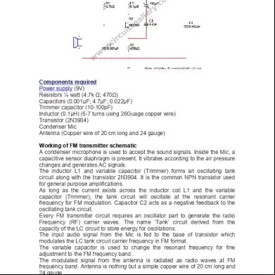
Fm Transmitter Circuit Diagram 5x6e6l
December 2019 57More Documents from "kuldeep Singh" 75ub

Hypermesh 11.0 Ls-dyna Tutorials 4l5r54
December 2021 0
Oracle Database 12c Sql Workshop 2 - Student Guide Volume 1.pdf 583g3g
October 2019 734
Secrets Of Yantra Mantra And Tantra By L R Chawdhri 5l3wt
November 2019 676
Drafting And Pleading Notes x4w4r
December 2019 156
Project Report On Fm Transmitter Andreceiver 622fe
October 2021 0