Pmma Data Sheet 39i30
This document was ed by and they confirmed that they have the permission to share it. If you are author or own the copyright of this book, please report to us by using this report form. Report 2z6p3t
Overview 5o1f4z
& View Pmma Data Sheet as PDF for free.
More details 6z3438
- Words: 2,120
- Pages: 8
MCC PRODUCT ATTRIBUTES
NANO PMMA and Copolymer
• Submicron linewidth control
PMMA (polymethyl methacrylate) is a versatile polymeric material that is well suited
• Sub 0.1µm imaging
for many imaging and non-imaging microelectronic applications. PMMA is most
™
commonly used as a high resolution positive resist for direct write e-beam as well as • E-beam, X-ray & deep UV imaging
x-ray and deep UV microlithographic processes. PMMA is also used as a protective
• Broad range of molecular weights & dilutions
coating for wafer thinning, as a bonding adhesive and as a sacrificial layer.
• Excellent adhesion to most substrates • Compatible with multi-layer processes
Standard PMMA products cover a wide range of film thicknesses and are formulated with 495,000 & 950,000 molecular weight (MW) resins in either chlorobenzene or the safer solvent anisole. Custom MW products ranging from 50,000 - 2.2 million are available upon request. In addition, we offer copolymer (MMA (8.5) MAA) products formulated in the safer solvent ethyl lactate. All MCC PMMA and copolymer resists
APPLICATIONS • Multi-layer T-gate processing
are available in package sizes from 500ml to 20 liters.
courtesy M/A Com
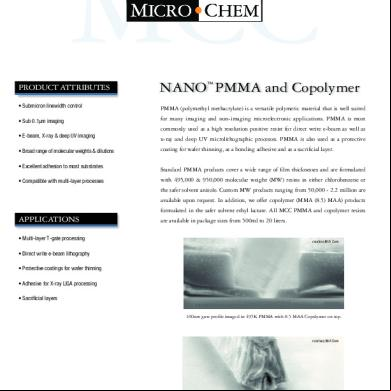
• Direct write e-beam lithography • Protective coatings for wafer thinning • Adhesive for X-ray LIGA processing • Sacrificial layers 100nm gate profile imaged in 495K PMMA with 8.5 MAA Copolymer on top.
courtesy M/A Com
T-gate resulting from PMMA/Copolymer bilayer resist stack.
PROCESSING GUIDELINES Typical process flow for bi-layer T-gate process
Substrate Preparation The substrate should be clean and dry. Solvent, O2 plasma, and O3
1.
2.
Spin Coat Bottom Layer PMMA Resist
cleans are commonly used and recommended.
Prebake PMMA
Coat MicroChem PMMA resists produce low defect coatings over a broad range of film thicknesses. The film thickness vs. spin-speed curves displayed in Fig. 1 through 8 provide the information required to select the appropriate PMMA dilution and spin speed needed to achieve the desired film thickness.
3.
4.
Spin Coat Top Layer Copolymer Resist
Remove Resist Edge Bead
The recommended coating conditions are: (1) Dispense: STATIC
5 - 8ml for a 150mm wafer
(2) Spread:
DYNAMIC
500 rpm for 5 sec OR
STATIC
0 rpm for 10 sec
(3) Spin:
Ramp to final spin speed at a high acceleration
5.
rate and hold for a total of 45 seconds.
6.
Expose and Develop Resist Stack
Prebake Copolymer
Pre Bake PMMA Hot plate:
180oC for 60 - 90 sec OR
Convection Oven:
170oC for 30 min 7.
Copolymer Hot plate:
150oC for 60 - 90 sec OR
Convection Oven:
140oC for 30 min
*Vacuum oven bake can also be used
8.
Gate Etch and Deposition
Strip/Remove Resist Stack
Expose
Table 2 outlines helpful guidelines for a develop process.
PMMA can be exposed with various parts of the electromagnetic
TYPICAL DEVELOPMENT PROCESS
spectrum. ACTION
SPRAY**
SPRAY PUDDLE
Dispense
500 rpm for 30-45 secs
500 rpm for 3-4 secs
IMMERSION (21OC)
e-beam: Dose - 50 - 500 µC/cm 2 depending on radiation source/equipment & developer used.
Dispense
0 rpm for 2 secs
Energy – 20-50kV; higher kV for higher resolution, e.g. 50kV for
No Dispense
0 rpm for 25-40 secs
30 secs
0.1mm images.
Rinse *
500 rpm for 30-45 secs
500 rpm for 3-4 secs
30 secs
Dry
500 rpm for 30 secs
5000 rpm for 30 secs
Nitrogen blow dry
DUV(deep UV): Low sensitivity, requiring doses >500mJ/cm 2 * Recommended Rinse solution is MIBK to IPA 1:3 in order to reduce the possibility of scumming
at 248nm.
** Variables such as developer pressure, nozzle type & position, spray pattern, etc. should be optimized
X-ray: Sensitivity of PMMA is low, ~1-2 J/cm2 at 8.3Å. The
Table 2
sensitivity increases at longer x-ray wavelengths. Features of <0.02µm can be fabricated.
Postbake/Hardbake (optional) To remove residual developer, rinse solvent, and moisture from the
Develop PMMA and copolymer resists are compatible with immersion (21oC), spray puddle, and spray process modes. Process variables such as soft bake, exposure conditions, choice of resist and developer should be optimized to achieve desired results. For more process details see the PMMA and Copolymer DEVELOPER
resist image. Hot Plate OR
100oC for 60 - 90 sec
Convection Oven
95oC for 30 min
Note: PMMA images will round/flow above 125oC.
data sheet. Table 1 lists commonly used developers and their
Remove
recommended usage.
NANOTM PMMA AND COPOLYMER DEVELOPERS ARE AVAILABLE IN THE FOLLOWING BLENDS PRODUCT
COMPOSITION
RESOLUTION
Wet:
Remover PG or ACRYL STRIP
Bath:
time as required, ambient
Spray:
time as required, 500 - 1000 rpm
Dry:
plasma O2
SENSITIVITY / THROUGHPUT
PMMA and copolymer resists can be removed by using MCC's M/I 1:1
1:1 MIBK to IPA
high
high
M/I 1:2
1:2 MIBK to IPA
higher
medium
M/I 1:3
1:3 MIBK to IPA
very high
low
MIBK
low
high
MIBK
Remover PG or standard cleanroom solvents, such as acetone, photoresist thinner, or positive photoresist removers. Resists that have seen higher processing temperatures and/or hostile processes that have toughened the polymer will require ACRYL STRIP or a more aggressive removal process. This can
Table 1
include Remover PG at elevated temperature followed by cleaner baths to assure adequate material removal.
Rinse and Dry To terminate the develop process and prevent scumming, PMMA
See appropriate product data sheet for specific process recom-
and copolymer should be immersed or sprayed with 1:3 or 1:4
mendations and safety precautions.
MIBK:IPA, alcohol or DI water immediately following develop. Substrates are normally spin dried at 3000rpm for 20 seconds or
For additional questions or technical assistance please
N2 blow dried.
Technical Services.
SPIN SPEED CURVES FOR PMMA AND COPOLYMER RESISTS The spin speed versus film thickness curves displayed in figures 1-11 provide approximate information required to select the appropriate PMMA or copolymer resist and spin conditions needed to obtain the desired film thickness. Actual results will vary and are equipment, environment, process and application specific. Additional resist dilutions to obtain other film thicknesses are available upon request.
10000 9000 8000 7000 6000 5000 4000 3000 2000 1000 0
495PMMA A Resists Solids: 2% - 6% in Anisole 7000 6000 Film Thickness (Å)
Film Thickness (Å)
495PMMA C Resists Solids: 2% - 6% in Chlorobenzene
C6
C4
5000 4000 A6
3000 2000
A4
1000
C2
A2
0 500
1000
1500
2000
2500
3000
3500
4000
500
4500
1000
1500
2000
2500
3000
3500
Spin Speed (rpm)
Spin Speed (rpm)
Figure 1
Figure 3
495PMMA C Resists Solids: 8% - 9% in Chlorobenzene
495PMMA A Resists Solids: 8% - 11% in Anisole
4000
4500
Film Thickness (Å)
C9
20000 15000 10000 A11 5000
A8
C8 0 500
1000
1500
2000
2500
3000
3500
4000
500
4500
1000
1500
2000
2500
3000
Spin Speed (rpm)
Spin Speed (rpm)
Figure 2
Figure 4
Copolymer Resists Solids: 6% - 11% in Ethyl Lactate 12000
Film Thickness, (Å)
Film Thickness (Å)
25000 23000 21000 19000 17000 15000 13000 11000 9000 7000 5000
10000 8000 6000 EL 11
4000 EL 9
2000 EL 6
0 500
1000
1500
2000
2500
Spin Speed (rpm)
Figure 9
3000
3500
4000
4500
3500
4000
4500
950PMMA A Resists Solids: 9% - 11% in Anisole
55000 50000 45000 40000 35000 30000 25000 20000 15000 10000
C10 C9
500
1000
1500
2000
2500
3000
3500
4000
55000 50000 45000 40000 35000 30000 25000 20000 15000 10000
Film Thickness (Å)
Film Thickness (Å)
950PMMA C Resists Solids: 9% - 10% in Chlorobenzene
A11 A9 500
4500
1000
1500
2000
950PMMA C Resists Solids: 2% - 7% in Chlorobenzene
3500
4000
4500
950PMMA A Resists Solids: 2% - 7% in Anisole 12000
25000
10000
20000 Film Thickness (Å)
Film Thickness (Å)
3000
Figure 7
Figure 5
15000 10000
C7
5000
C4
0 500
2500
Spin Speed (rpm)
Spin Speed (rpm)
C2 1000
1500
2000
2500
3000
3500
4000
8000 6000 4000
A7
2000
A4
4500
A2
0 500
Spin Speed (rpm)
1000
1500
2000
2500
3000
3500
4000
4500
Spin Speed (rpm)
Figure 6
Figure 8
Optical Properties Copolymer Resists
Optical Properties 495 and 950 PMMA Resists 1.7
1.7
Cauchy Coeffiecients A 495 PMMA 950 PMMA
1.491 1.488
3.427 e-03 2.898 e-03
Cauchy Coeffiecients A
C 1.65
1.819 e-04 1.579 e-04
Refractive Index
Refractive Index
1.65
B
1.6
1.55
1.5
8.5 mEL
1.478
B
C
7.204 e-04
-3.478 e-04
1.6
1.55
1.5
1.45 0
300
500
700
Wavelength (nm)
Figure 10
900
1.45 0
300
500
700
Wavelength (nm)
Figure 11
900
Bi-Layer Process
PMMA resists for T-gate and other imaging processes PMMA is a high resolution positive tone resist for e-beam, deep UV
PMMA
PMMA
GaAs
GaAs
4. Develop PMMA and Copolymer
1. Coat and bake PMMA
(200-250nm) and X-ray lithographic processes. Although PMMA may be used in a single layer resist process, it is most commonly used in
Copolymer PMMA
multi-layer processes such as in the fabrication of mushroom or T-gates. Images are formed through the photo scission of the polymer backbone and subsequent development process, which
5. Deposition
e-beam >>
removes the exposed, lower molecular weight resist. Multi-layer,
GaAs
GaAs
2. Coat and bake copolymer
PMMA
shaped resist profiles are realized and influenced through the careful choice of PMMA molecular weight, film thickness and other process
GaAs
3. Expose resist stack, center scan dose, then side scan dose
GaAs
6. Strip resist stack
set points.
Tri-Layer Process
In a typical bi-layer process, a combination of bottom and top layer resists are selected such that a large difference in dissolution rates
PMMA
PMMA Copolymer PMMA
GaAs
GaAs
1. Coat and bake high MW PMMA
5. Develop tri-layer stack
of the layers at the developer step exists, leading to the desired resist sidewall profile. This contrast may be further influenced with a PMMA
PMMA Copolymer PMMA
GaAs
GaAs
Copolymer
variety of process strategies. Generally, dissolution rate increases as molecular weight decreases. However, soft bake conditions, which
2. Coat and bake copolymer
6. Deposition
affect residual solvent level and subsequent development rates will influence the bi-layer resist profile as will the exposure conditions.
PMMA Copolymer PMMA
3. Coat and bake low MW PMMA
7. Strip resist stack
notes concerning non-imaging PMMA processes such as wafer e-beam >>
thinning, bonding and sacrificial layers.
GaAs
GaAs
Please refer to our web site, www.microchem.com for applications
PMMA Copolymer PMMA GaAs
4. Expose resist stack, center scan dose, then side scan dose
OTHER RESIST AND ANCILLORY PRODUCTS FROM MICROCHEM PMGI and LOR for lift-off processing SU-8 resists for MEMS and ultra thick resist processing Remover PG resist stripper EBR PG edge bead remover Acryl Strip resist stripper for PMMA
NOTES
HANDLING NANO PMMA & COPOLYMER SERIES RESISTS (in Anisole or Chlorobenzene) Use precautions in handling flammable PMMA solutions. Avoid with eyes, skin, and clothing. Use with adequate ventilation. Avoid breathing fumes. Wear chemical-resistant eye protection, chemical gloves (PVA for chlorobenzene solutions) and protective clothing when handling NANO PMMA & Copolymer Series Resist products. NANO PMMA & Copolymer Series Resists cause irritation in case of with eyes, skin, and mucous membranes. In case of eye , flush with water for 15 minutes and call a physician immediately. Review the current MSDS (Material Safety Data Sheet) before using.
MATERIAL AND EQUIPMENT COMPATIBILITY NANO PMMA & Copolymer Resists are compatible with glass, ceramic, unfilled polyethylene, high-density polyethylene, polytetrafluoroethylene, stainless steel, and equivalent materials. Chlorobenzene is a powerful solvent and will attack various elastomers such as BUNA N, EPDM, HYPALON, and NEOPRENE. It will also attack PVC, VC and polyester. VITON A is recommended for both O-rings and tubing.
PROCESSING ENVIRONMENT For optimum results, use NANO PMMA & Copolymer Series Resists in a controlled environment. 20 - 25o ±1oC (68 - 77oF) is suggested.
STORAGE Store upright in original containers in a dry area above 50oF. Do not refrigerate. Keep away from sources of ignition, light, heat, oxidants, acids, and reducers. Shelf life is 13 months from date of manufacture.
DISPOSAL Each locality, state, and county has unique regulations regarding the disposal of organic solvents such as NANO PMMA Series Resists. It is the responsibility of the customer to dispose of NANO PMMA Series Resists in compliance with all applicable codes and regulations. See MSDS for additional information.
1254 C HESTNUT S TREET N EWTON , MA 02464 P HONE : 617.965.5511 F AX : 617.965.5818 E MAIL :
[email protected]
The information regarding these products is based on our testing to date, which we believe to be reliable, but accuracy or completeness is not guaranteed. We make no guarantee or warranty, expressed or implied, regarding the information, use, handling, storage, or possession of these products, or the application of any process described herein or the results desired, since the use and handling of these products are beyond our control.
WWW.MICROCHEM.COM © MicroChem Corp. copyright 2001. All rights reserved. LOR is a trademark of MicroChem Corp.
