Datasheet 2p235m
This document was ed by and they confirmed that they have the permission to share it. If you are author or own the copyright of this book, please report to us by using this report form. Report 2z6p3t
Overview 5o1f4z
& View Datasheet as PDF for free.
More details 6z3438
- Words: 1,770
- Pages: 13
HCC/HCF4093B QUAD 2-INPUT NAND SCHMIDT TRIGGERS
. . . .. . .. ..
SCHMITT-TRIGGER ACTION ON EACH INPUT WITH NO EXTERNAL COMPONENTS HYSTERESIS VOLTAGE TYPICALLY 0.9V AT VDD = 5V AND 2.3V AT VDD = 10V NOISE IMMUNITY GREATER THAN 50% OF VDD (typ.) NO LIMIT ON INPUT RISE AND FALL TIMES STANDARDIZED SYMMETRICAL OUTPUT CHARACTERISTICS QUIESCENT CURRENT SPECIFIED TO 20V FOR HCC DEVICE 5V, 10V, AND 15V PARAMETRIC RATINGS INPUT CURRENT OF 100nA AT 18V AND 25°C FOR HCC DEVICE 100% TESTED FOR QUIESCENT CURRENT MEETS ALL REQUIREMENTS OF JEDEC TENTATIVE STANDARD N°. 13A, ”STANDARD SPECIFICATIONS FOR DESCRIPTION OF ”B” SERIES CMOS DEVICES”
EY (Plastic Package)
M1 (Micro Package)
F (Ceramic Frit Seal Package)
C1 (Plastic Chip Carrier)
ORDER CODES : HCC4093BF HCF4093BM1 HCF4093BEY HCF4093BC1
PIN CONNECTIONS
DESCRIPTION The HCC4093B (extended temperature range) and HCF4093B (intermediate temperature range) are available in 14-lead dual in-line plastic or ceramic package and plastic micropackage. The HCC/HCF4093B consists of four Schmitt-trigger circuits. Each circuit functions as a two-input NAND gate with Schmitt-trigger action on both inputs. The gate switches at different points for positive and negative-going signals. The difference between the positive voltage (VP) and the negative voltage (VN) is defined as hysteresis voltage (VH) (see fig. 1). June 1989
1/13
HCC/HCF4093B FUNCTIONAL DIAGRAM 1 of 4 Schmitt triggers
ABSOLUTE MAXIMUM RATINGS Symbol V DD *
Parameter Supply Voltage : HC C Types H C F Types
Value
Unit
– 0.5 to + 20 – 0.5 to + 18
V V
– 0.5 to V DD + 0.5
V
VI
Input Voltage
II
DC Input Current (any one input)
± 10
mA
Pto t
Total Power Dissipation (per package) Dissipation per Output Transistor for T o p = Full Package-temperature Range
200
mW
100
mW
T op
Operating Temperature : HCC Types H CF Types
– 55 to + 125 – 40 to + 85
°C °C
T stg
Storage Temperature
– 65 to + 150
°C
Stresses above those listed under ”Absolute Maximum Ratings ”may cause permanent damage to the device. This is a stress rating only and functional operation of the device at these or any other conditions above those indicated in the operational sections of this specification is not implied. Exposure to absolute maximum rating conditions for external periods may affect device reliability. * All voltage values are referred to VSS pin voltage.
RECOMMENDED OPERATING CONDITIONS Symbol V DD VI Top
2/13
Parameter Supply Voltage : HC C Types H CF Types Input Voltage Operating Temperature : HCC Types H CF Types
Value
Unit
3 to 18 3 to 15
V V
0 to V DD
V
– 55 to + 125 – 40 to + 85
°C °C
HCC/HCF4093B STATIC ELECTRICAL CHARACTERISTICS (over recommended operating conditions) Symbol IL
Parameter Quiescent Current
HCC Types
HCF Types VP
VN
VH
V OH
V OL
I OH
Positive Trigger Threshold Voltage
Negative Trigger Threshold Voltage
Hysteresis Voltage
Output High Voltage Output Low Voltage Output Drive Current
HCC Types
HCF Types a b * *
Test Conditions VO |I O | V D D VI (V) (V) (µA) (V) 0/ 5 5 0/10 10 0/15 15 0/20 20 0/ 5 5 0/10 10 0/15 15 a 5 a 10 a 15 b 5 b 10 b 15 a 5 a 10 a 15 b 5 b 10 b 15 a 5 a 10 a 15 b 5 b 10 b 15 0/ 5 < 1 5 0/10 < 1 10 0/15 < 1 15 5/0 < 1 5 10/0 < 1 10 15/0 < 1 15 0/ 5 2.5 5 0/ 5 4.6 5 0/10 9.5 10 0/15 13.5 15 0/ 5 2.5 5 0/ 5 4.6 5 0/10 9.5 10 0/15 13.5 15
T L o w* Min. Max. 1 2 4 20 4 8 16 2.2 3.6 4.6 7.1 6.8 10.8 2.6 4 5.6 8.2 6.3 12.7 0.9 2.8 2.5 5.2 4 7.4 1.4 3.2 3.4 6.6 4.8 9.6 0.3 1.6 1.2 3.4 1.6 5 0.3 1.6 1.2 3.4 1.6 5 4.95 9.95 14.95 0.05 0.05 0.05 –2 – 0.64 – 1.6 – 4.2 – 1.53 – 0.52 – 1.3 – 3.6
Value 25 °C T Hi g h * Min. Typ. Max. Min. Max. 0.02 1 30 0.02 2 60 0.02 4 120 0.04 20 600 0.02 4 30 0.02 8 60 0.02 16 120 2.2 2.9 3.6 2.2 3.6 4.6 5.9 7.1 4.6 7.1 6.8 8.8 10.8 6.8 10.8 2.6 3.3 4 2.6 4 5.6 7 8.2 5.6 8.2 6.3 9.4 12.7 6.3 12.7 0.9 1.9 2.8 0.9 2.8 2.5 3.9 5.2 2.5 5.2 4 5.8 7.4 4 7.4 1.4 2.3 3.2 1.4 3.2 3.4 5.1 6.6 3.4 6.6 4.8 7.3 9.6 4.8 9.6 0.3 0.9 1.6 0.3 1.6 1.2 2.3 3.4 1.2 3.4 1.6 3.5 5 1.6 5 0.3 0.9 1.6 0.3 1.6 1.2 2.3 3.4 1.2 3.4 1.6 3.5 5 1.6 5 4.95 4.95 9.95 9.95 14.95 14.95 0.05 0.05 0.05 0.05 0.05 0.05 – 1.6 – 3.2 – 1.15 – 0.51 – 1 – 0.36 – 1.3 – 2.6 – 0.9 – 3.4 – 6.8 – 2.4 – 1.36 – 3.2 – 1.1 – 0.44 – 1 – 0.36 – 1.1 – 2.6 – 0.9 – 3.0 – 6.8 – 2.4
Unit
µA
V
V
V
V
V
mA
: input on terminals 1, 5, 8, 12 or 2, 6, 9, 13 ; other inputs to VDD. : input on terminals 1 and 2, 5 and 6, 8 and 9, or 12 and 13 ; other inputs to VDD . TLo w = –55°C for HCC device : -40°C for HCF device. THigh = +125°C for HCC device : +85°C for HCF device.
3/13
HCC/HCF4093B STATIC ELECTRICAL CHARACTERISTICS ( continued) Test Conditions Symbol
I OL
I IH , I IL
CI
Parameter
Output Sink Current
Input Leakage Current
VI (V)
VO (V)
Value
|I O | V D D T L o w* 25 °C T Hi g h * (µA) (V) Min. Max. Min. Typ. Max. Min. Max.
0/ 5
0.4
5
0.64
0.51
1
0.36
0/10
0.5
10
1.6
1.3
2.6
0.9
0/15
1.5
15
4.2
3.4
6.8
2.4
0/ 5
0.4
5
0.52
0.44
1
0.36
0/10
0.5
10
1.3
1.1
2.6
0.9
0/15
1.5
15
3.6
3.0
6.8
2.4
HCC 0/18 Types HCF 0/15 Types
Input Capacitance
mA
18
± 0.1
± 10- 5 ± 0.1
±1
15
± 0.3
± 10
± 1
Any Input
Any Input
5
-5
± 0.3
Unit
7.5
µA
pF
DYNAMIC ELECTRICAL CHARACTERISTICS (T amb = 25°C, C L = 50pF, R L = 200kΩ, typical temperature coefficient for all V DD = 0.3%/°C values , all input rise and fall time = 20ns) Symbol
Parameter
Test Conditions V D D (V) Min.
t P L H , t P HL Propagation Delay Time
t TL H, t T HL
Value
Transition Time
Typ.
Max.
5
190
380
10
90
180
15
65
130
5
100
200
10
50
100
15
40
80
Figure1 : Hysteresis Definition, Characteristics and Test Setup. (a) Definition of VP, VN and VH
4/13
(b) Transfer characteristics of 1 of 4 gates
Unit
ns
ns
HCC/HCF4093B (c) Test setup
Figure 2 : Input and Output Characteristics.
Figure 3 : Typical Current and Voltage Transfer Characteristics.
Figure 4 : Typical Voltage Transfer Characteristics as a Function of Temperature, and Test Circuit.
5/13
HCC/HCF4093B Figure 5 : Typical Output Low (sink) Current Characteristics.
Figure 6 : Minimum Output Low (sink) Current Characteristics.
Figure 7 : Typical Output High (source) Current Characteristic.
Figure 8 : Minimum Output High Current Characteristics.
Figure 9 : Typical Propagation Delay Time vs. Supply Voltage.
Figure 10 : Typical Transition Time vs. Load Capacitance.
6/13
HCC/HCF4093B Figure 11 : Typical Trigger Threshold Voltage vs.VDD
Figure 12 : Typical per cent Hysteresis vs. Supply Voltage.
Figure 13 : Typical Dissipation Characteristics.
Figure 14 : Power Dissipation vs. Rise and Fall Times.
7/13
HCC/HCF4093B APPLICATIONS Figure 15 : Wave Shaper.
Figure 16 : Monostable Multivibrator.
Figure17 : Astable Multivibrator.
TEST CIRCUITS Figure18 : Quiescent Device Current.
8/13
Figure 19 : Input Leakage Current.
HCC/HCF4093B
Plastic DIP14 MECHANICAL DATA mm
DIM. MIN. a1
0.51
B
1.39
TYP.
inch MAX.
MIN.
TYP.
MAX.
0.020 1.65
0.055
0.065
b
0.5
0.020
b1
0.25
0.010
D
20
0.787
E
8.5
0.335
e
2.54
0.100
e3
15.24
0.600
F
7.1
0.280
I
5.1
0.201
L Z
3.3 1.27
0.130 2.54
0.050
0.100
P001A
9/13
HCC/HCF4093B
Ceramic DIP14/1 MECHANICAL DATA mm
DIM. MIN.
TYP.
inch MAX.
MIN.
TYP.
MAX.
A
20
0.787
B
7.0
0.276
D E
3.3
0.130
0.38
e3
0.015 15.24
0.600
F
2.29
2.79
0.090
0.110
G
0.4
0.55
0.016
0.022
H
1.17
1.52
0.046
0.060
L
0.22
0.31
0.009
0.012
M
1.52
2.54
0.060
0.100
N P Q
10.3 7.8
8.05 5.08
0.406 0.307
0.317 0.200
P053C
10/13
HCC/HCF4093B
SO14 MECHANICAL DATA mm
DIM. MIN.
TYP.
A a1
inch MAX.
MIN.
TYP.
1.75 0.1
0.068
0.2
a2
MAX.
0.003
0.007
1.65
0.064
b
0.35
0.46
0.013
0.018
b1
0.19
0.25
0.007
0.010
C
0.5
0.019
c1
45° (typ.)
D
8.55
E
5.8
8.75
0.336
6.2
0.228
0.344 0.244
e
1.27
0.050
e3
7.62
0.300
F
3.8
4.0
0.149
0.157
G
4.6
5.3
0.181
0.208
L
0.5
1.27
0.019
0.050
M S
0.68
0.026 8° (max.)
P013G
11/13
HCC/HCF4093B
PLCC20 MECHANICAL DATA mm
DIM. MIN.
TYP.
inch MAX.
MIN.
TYP.
MAX.
A
9.78
10.03
0.385
0.395
B
8.89
9.04
0.350
0.356
D
4.2
4.57
0.165
0.180
d1
2.54
0.100
d2
0.56
0.022
E
7.37
8.38
0.290
0.330
e
1.27
0.050
e3
5.08
0.200
F
0.38
0.015
G
0.101
0.004
M
1.27
0.050
M1
1.14
0.045
P027A
12/13
HCC/HCF4093B
Information furnished is believed to be accurate and reliable. However, SGS-THOMSON Microelectronics assumes no responsability for the consequences of use of such information nor for any infringement of patents or other rights of third parties which may results from its use. No license is granted by implication or otherwise under any patent or patent rights of SGS-THOMSON Microelectronics. Specifications mentioned in this publication are subject to change without notice. This publication supersedes and replaces all information previously supplied. SGS-THOMSON Microelectronics products are not authorized for use ascritical components in life devices or systems without express written approval of SGS-THOMSON Microelectonics. 1994 SGS-THOMSON Microelectronics - All Rights Reserved SGS-THOMSON Microelectronics GROUP OF COMPANIES Australia - Brazil - - - Hong Kong - Italy - Japan - Korea - Malaysia - Malta - Morocco - The Netherlands Singapore - Spain - Sweden - Switzerland - Taiwan - Thailand - United Kingdom - U.S.A
13/13
Related Documents c2h70

Datasheet 2p235m
February 2023 0
Datasheet 2p235m
July 2022 0
Datasheet 2p235m
August 2022 0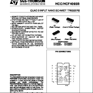
Datasheet 2p235m
November 2019 191
Datasheet 2p235m
October 2022 0
Datasheet 2p235m
October 2022 0More Documents from "Jesus Cardenas Bermudez" 205l20
Datasheet 2p235m
November 2019 191
Desafectacion De Bien Mueble 2x3oi
July 2020 0
6g3p1u
December 2019 37
Bomba C101-c102.pdf 652c4x
December 2019 47
Manual Sany Mantenimiento 2m3t5i
October 2020 0