Datasheet 2p235m
This document was ed by and they confirmed that they have the permission to share it. If you are author or own the copyright of this book, please report to us by using this report form. Report 2z6p3t
Overview 5o1f4z
& View Datasheet as PDF for free.
More details 6z3438
- Words: 4,709
- Pages: 13
Ordering number : EN*A1630
Thick-Film Hybrid IC
STK433-290-E
3-channel class AB audio power IC, 80W+80W+80W
Overview The STK433-290-E is a hybrid IC designed to be used in 80W × 3ch class AB audio power amplifiers.
Applications • Audio power amplifiers.
Features • Pin-to-pin compatible outputs ranging from 80W to 150W. • Can be used to replace the STK433-000/-100 series (30W to 150W × 2ch) and STK433-200(A) series (30W to 60W × 3ch) due to its pin compatibility. • Miniature package (64.0mm × 36.6mm × 9.0mm) • Output load impedance: RL = 6Ω to 4Ω ed • Allowable load shorted time: 0.3 second • Allows the use of predesigned applications for standby and mute circuits.
Series Models STK433-290-E
STK433-300-E
STK433-320-E
STK433-330-E
Output 1 (10%/1kHz)
80W×3ch
100W×3ch
120W×3ch
150W×3ch
Output 2 (0.4%/20Hz to 20kHz)
50W×3ch
60W×3ch
80W×3ch
100W×3ch
Maximum rating VCC max (no sig.)
±54V
±57V
±65V
±71.5V
Maximum rating VCC max (6Ω)
±47V
±50V
±57V
±63V
Recommended operating VCC (6Ω)
±33V
±36V
±41V
±44V
Dimensions (excluding pin height)
64.0mm×36.6mm×9.0mm
Any and all SANYO Semiconductor Co.,Ltd. products described or contained herein are, with regard to "standard application", intended for the use as general electronics equipment (home appliances, AV equipment, communication device, office equipment, industrial equipment etc.). The products mentioned herein shall not be intended for use for any "special application" (medical equipment whose purpose is to sustain life, aerospace instrument, nuclear control device, burning appliances, transportation machine, traffic signal system, safety equipment etc.) that shall require extremely high level of reliability and can directly threaten human lives in case of failure or malfunction of the product or may cause harm to human bodies, nor shall they grant any guarantee thereof. If you should intend to use our products for applications outside the standard applications of our customer who is considering such use and/or outside the scope of our intended standard applications, please consult with us prior to the intended use. If there is no consultation or inquiry before the intended use, our customer shall be solely responsible for the use. Specifications of any and all SANYO Semiconductor Co.,Ltd. products described or contained herein stipulate the performance, characteristics, and functions of the described products in the independent state, and are not guarantees of the performance, characteristics, and functions of the described products as mounted in the customer' s products or equipment. To symptoms and states that cannot be evaluated in an independent device, the customer should always evaluate and test devices mounted in the customer' s products or equipment.
21710HKIM No. A1630-1/13
STK433-290-E Specifications Absolute maximum ratings at Ta=25°C, Unless otherwise specified Tc=25°C Parameter
Symbol
Conditions
Ratings
Unit ±54
V
Maximum power supply voltage
VCC max (0)
Non signal
Maximum power supply voltage
VCC max (1)
RL≥6Ω
Minimum operating supply voltage
VCC min
#13 Operating voltage
VST OFF max
Thermal resistance
θj-c
Per one power transistor
2.1
Junction temperature
Tj max
Should satisfy Tj max and Tc max
150
°C
Operating substrate temperature
Tc max
125
°C
Storage temperature
Tstg
-30 to +125
°C
Allowable time for load short-circuit
ts
±47
V
±10
V
-0.3 to +5.5
V
VCC=±33V, RL=6Ω, f=50Hz, PO=50W,
°C/W
0.3
1-channel active
s
Operating Characteristics at Unless otherwise specified Tc=25°C, RL=6Ω (Non-inductive Load), Rg=600Ω, VG=30dB Conditions *2 Parameter
Symbol PO (1)
±33
20 to 20k
0.4
PO (2)
±33
1k
10
THD (1)
±33
20 to 20k
THD (2)
±33
1k
Frequency characteristics *1
fL, fH
±33
Input impedance
ri
±33
VNO
±39
Rg=2.2kΩ
ICCO
±39
No loading
Total harmonic distortion
Output noise voltage
*1
*1
*3
Quiescent current Output neutral voltage #13 Stand-by ON threshold
*5
#13 Stand-by OFF threshold *5
PO (W)
unit
(Hz)
Output power
f
Ratings
VCC (V)
THD
5.0
typ
47
max
50
W
80 0.4
VG=30dB
%
0.01 1.0
1k
min
(%)
+0 -3dB
20 to 50k
1.0
Hz
55
VN
±39
VST ON
±33
Stand-by
VST OFF
±33
Operation
kΩ 1.0
mVrms
30
70
120
mA
-70
0
+70
mV
0
0.6
2.5
3.0
V V
[Remarks] *1: For 1-channel operation *2: Unless otherwise specified, use a constant-voltage power supply to supply power when inspections are carried out. *3: The output noise voltage values shown are peak values read with a VTVM. However, an AC stabilized (50Hz) power supply should be used to minimize the influence of AC primary side flicker noise on the reading. *4: Use the transformer power supply circuit shown in the figure below for allowable load shorted time and output noise voltage measurement. *5: The impression voltage of ‘#13 (Stand-By) pin’ must not exceed the maximum rating. Power amplifier operate by impressing voltage +2.5 to +5.5V to ‘#13 (Stand-By) pin’. *6: Please connect -PreVCC pin (#1 pin)with the stable minimum voltage, and connect so that current does not flow in by reverse bias. *7: Thermal design must be implemented based on the conditions under which the customer’s end products are expected to operate on the market. *8: The case of this Hybrid-IC is using thermosetting silicon adhesive (TSE322SX). *9: Weight of HIC: 24.8g Outer carton dimensions (W×L×H): 452mm×325mm×192mm
DBA40C
10000μF +VCC
+
Designated transformer power supply (MG-200 equivalent)
500Ω + 500Ω -VCC 10000μF
No. A1630-2/13
STK433-290-E Package Dimensions unit:mm (typ) 64.0 (R1.8)
9.0
19 2.9
4.0
1
25.8
18.7
5.0
36.6
55.6
3.6 2.0 (9.8)
0.4
0.5
18 2.0=36.0
5.5
RoHS DIRECTIVE
Equivalent Circuit
3
8
Pre Driver CH3
Pre Driver CH2
Pre Driver CH1
MONO IC 11
+
+
+
12
-
-
-
Bias Circuit 1 2
SUB 9
5 4 6 7
10
13
14 15 16 17
19 18
No. A1630-3/13
STK433-290-E Application Circuit STK433-300sr Ch1 -PRE -VCC +VCC OUT 1
2
3
Ch1 Ch1 Ch2 Ch2 OUT OUT OUT +PRE SUB GND IN
4
6
5
7
8
9
10
Ch1 NF
11
12
ST- Ch2 BY NF 13
14
Ch2 Ch3 IN IN 15
16
Ch3 NF 17
Ch3 Ch3 OUT OUT 18
R22
R21
R20
19
C19
R08
C20
R30
C21
Stand-by Control R10
C10 R09
C06
C12
Ch3 IN C05
C11 R11
R12
R13
C13
C14
C15
R04
R03
R06
C08
R05
C07
R07
C09 Ch2 IN Ch2 IN
GND
R23
Ch1 IN C04
R02 L03 Ch3 OUT
R01 C23
C03
L02
R16
C18 R19 Ch2 OUT
C17
C01 R15
R18 GND
GND
GND GND
C02 R17 L01
C16
Ch1 OUT
R14
PCB Layout Example
C23
No. A1630-4/13
STK433-290-E Recommended External Components Parts
Recommended
Location
value
R01, R23
100Ω/1W
Circuit purpose
Above Recommended
Below Recommended
value
value
Resistance for ripple filter.
Short-through current
(Fuse resistance is recommended. Ripple filter is
-
may increase at high
constituted with C03, C23.)
frequency.
R02, R03, R04
1kΩ
Resistance for input filters.
R05, R06, R07
56kΩ
Input impedance is determined.
R08, R09, R10
56kΩ
Voltage gain (VG) is determined with R11, R12, R13
R11, R12, R13
1.8kΩ
Voltage gain (VG) is determined with R8, R9, R10.
It may oscillate.
With especially no
(As for VG, it is desirable to set up by R11, R12, R13.)
(VG<30dB)
problem
R14, R15, R16
4.7Ω
Noise absorption resistance.
-
-
R17, R18, R19
4.7Ω/1W
Resistance for oscillation prevention.
-
-
-
-
Output neutral voltage (VN) shift. (It is referred that R05=R08, R06=R09, R07=R10)
R20, R21, R22
-
-
0.22Ω
Output emitter resistor
Decrease of maximum
It may cause thrmal
±10%, 5W
(Metal-plate resistor is recommended.)
output Power
runaway
R30
Note*5
Select restriction resistance, for the impression voltage of ‘#17 (Stand-By) pin’ must not exceed the maximum
C01, C02
100μF/100V
Capacitor for oscillation prevention.
rating. • Locate near the HIC as much as possible. • Power supply impedance is lowered and stable
-
-
operation of the IC is carried out. (Electrolytic capacitor is recommended.) C03, C23
100μF/100V
Decoupling capacitor
The change in the ripple ingredient mixed in an input
• The ripple ingredient mixed in an input side is removed
side from a power supply line
from a power supply line. (Ripple filter is constituted with R03, R04.) C04, C05, C06
2.2μF/50V
Input coupling capacitor. (for DC current prevention.)
C07, C08, C09
470pF
Input filter capacitor
-
• A high frequency noise is reduced with the filter
-
constituted by R02, R03, R04. C10, C11, C12
3pF
Capacitor for oscillation prevention.
It may oscillate.
C13, C14, C15
10μF/10V
Negative capacitor.
The voltage gain (VG)
The voltage gain (VG)
• The cutoff frequency of a low cycle changes.
of low frequency is
of low frequency
extended. However, the
decreases.
(fL=1/(2π ⋅ C13 ⋅ R11))
pop noise at the time of a power supply injection also becomes large. C16, C17, C18
0.1μF
Capacitor for oscillation prevention.
It may oscillate.
C19, C20, C21
68pF
Capacitor for oscillation prevention.
It may oscillate.
L01, L02, L03
3μH
Coil for oscillation prevention.
With especially
It may oscillate.
no problem
No. A1630-5/13
STK433-290-E STK433-100/-300sr PCB PARTS LIST PCB Name: STK403-000Sr/100Sr/200Sr PCBA Location No. (*2) 2ch Amp doesn't mount parts of ( ).
PARTS
RATING
-
-
Component c
Hybrid IC#1 Pin Position STK433-100Sr (*2)
STK433-300Sr
R01
ERG1SJ101
100Ω, 1W
enabled
R02, R03, (R04)
RN16S102FK
1kΩ, 1/6W
enabled
R05, R06, (R07), R08, R09, (R10)
RN16S563FK
56kΩ, 1/6W
enabled
R11, R12, (R13)
RN16S182FK
1.8kΩ, 1/6W
enabled
R14, R15, (R16)
RN14S4R7FK
4.7Ω, 1/4W
enabled
R17, R18, (R19)
ERX1SJ4R7
4.7Ω, 1W
enabled
R20, R21, (R22)
Metal-plate resistor is
0.22Ω, 5W
enabled
recommended C01, C02, C03, C23
(*3)
C04, C05, (C06)
100MV100HC
100μF, 100V
50MV2R2HC
2.2μF, 50V
enabled enabled (*1)
C07, C08, (C09)
DD104-63B471K50
470pF, 50V
enabled
C10, C11, (C12)
DD104-63CJ030C50
3pF, 50V
enabled
C13, C14, (C15)
10MV10HC
10μF, 10V
enabled (*1)
C16, C17, (C18)
ECQ-V1H104JZ
0.1μF, 50V
C19, C20, (C21)
DD104-63B***K50
***pF, 50V
R34, R35, (R36)
RN16S302FK
3kΩ, 1/6W
L01, L02, (L03)
-
68pF Short
3μH
enabled
VCE≥75V, IC≥1mA
enabled
GMB01(Reference)
Di
enabled
RN16S***FK
***kΩ, 1/6W
R31
RN16S333FK
33kΩ, 1/6W
enabled
R32
RN16S102FK
1kΩ, 1/6W
enabled
R33
RN16S202FK
2kΩ, 1/6W
enabled
C32
10MV33HC
33μF, 10V
Stand-By
Tr1
Control
D1
Circuit
enabled 100pF
R30
2SC3332 (Reference)
(*4)
13kΩ
2.7kΩ
enabled
J1, J2, J3, J4, J5, J6, J8, J9
-
-
enabled
J7, JS2, JS3, JS4, JS5, JS7, JS8, JS9
-
-
-
-
enabled
JS6, JS10 JS1
ERG1SJ101
100Ω, 1W
enabled
(*1) Capacitor mark “A” side is “-” (negative). (*2) STK433-100Sr (2ch AMP) doesn’t mount parts of ( ). (*3) Add parts C23 to the other side of PCB. (*4) Recommended standby circuit is used.
No. A1630-6/13
STK433-290-E Pin Assignments [STK433-000/-100/-200Sr & STK415/416-100Sr Pin Layout] 1
2ch class-AB
2
3
4
5
(Size) 47.0×25.6×9.0
6
7
8
9
10
11
12
13
14
15
I
N
S
N
I
N
F
T
F
N
2ch classAB/2.00mm
STK433-030-E 30W/JEITA
-
-
+
O
O
O
O
+
STK433-040-E 40W/JEITA
P
V
V
U
U
U
U
P
S
G
STK433-060-E 50W/JEITA
R
C
C
T
T
T
T
R
U
N
/
/
A
/
/
STK433-070-E 60W/JEITA
E
C
C
/
/
/
/
E
B
D
C
C
N
C
C
C
C
C
C
•
H
H
D
H
H
H
H
H
H
G
1
1
|
2
2
1
1
2
2
N
B
+
-
+
-
D
Y
7
15
(Size) 67.0×25.6×9.0 STK433-090-E 80W/JEITA STK433-100-E 100W/JEITA STK433-120-E 120W/JEITA STK433-130-E 150W/JEITA 1
2
3
4
5
6
STK433-230A-E 30W/JEITA
-
-
+
O
O
O
O
+
STK433-240A-E 40W/JEITA
P
V
V
U
U
U
U
P
S
G
STK433-260A-E 50W/JEITA
R
C
C
T
T
T
T
R
U
N
STK433-270-E 60W/JEITA
E
C
C
/
/
/
/
E
B
D
C
C
C
C
STK433-290-E 80W/JEITA
H
H
H
STK433-300-E 100W/JEITA
1
1
2
STK433-320-E 120W/JEITA
+
-
8
9
3ch class-AB (Size) 67.0×25.6×9.0
8
9
10
11
12
13
14
16
17
18
19
I
N
S
N
N
F
T
F
I
I
N
O
O
N
N
F
U
/
/
A
/
U
/
/
/
T
C
C
N
T
C
C
C
C
/
•
H
H
/
D
H
H
H
H
C
C
H
G
1
1
2
N
B
|
2
2
3
3
H
H
3
+
-
D
Y
3
+
-
10
11
3ch classAB/2.00mm
(Size) 64.0×36.6×9.0
STK433-330-E 150W/JEITA 2ch class-H
1
2
3
4
5
6
7
(Size) 64.0×31.1×9.0
12
13
14
15
16
17
18
19
I
N
S
N
I
N
F
T
F
N
2ch classH/2.00mm
STK415-090-E 80W/JEITA
+
-
+
-
-
-
+
O
O
O
O
+
STK415-100-E 90W/JEITA
V
V
O
O
P
V
V
U
U
U
U
P
S
G
STK415-120-E 120W/JEITA
L
L
H
H
T
T
T
T
R
U
N
/
/
A
/
/
/
/
/
/
E
B
D
C
C
N
C
C
F
F
R
STK415-130-E 150W/JEITA
F
F
E
STK415-140-E 180W/JEITA
S
S
C
C
C
C
•
H
H
D
H
H
E
E
H
H
H
H
G
1
1
|
2
2
T
T
1
1
2
2
N
3
4
19
3ch class-H
1
2
5
6
7
+
-
+
-
8
9
10
11
(Size) 64.0×31.1×9.0
B
D 12
13
Y 14
15
16
17
18
20
21
22
23
3ch classH/2.00mm
STK416-090-E 80W/JEITA
+
-
+
-
-
-
+
O
O
O
O
+
I
N
S
N
I
I
N
O
O
STK416-100-E 90W/JEITA
V
V
O
O
P
V
V
U
U
U
U
P
S
G
N
F
T
F
N
N
F
U
U
STK416-120-E 120W/JEITA
L
L
F
F
R
H
H
T
T
T
T
R
U
N
/
/
A
/
/
/
/
T
T
F
F
E
/
/
/
/
E
B
D
C
C
N
C
C
C
C
/
/
S
S
C
C
C
C
•
H
H
D
H
H
H
H
C
C
E
E
H
H
H
H
G
1
1
|
2
2
3
3
H
H
T
T
1
1
2
2
N
B
3
3
+
-
+
-
D
Y
+
-
STK416-130-E 150W/JEITA
No. A1630-7/13
STK433-290-E
THD - PO
Total power dissipation within the board, Pd - W
100 7 5 3 2
VCC=±33V RL=6Ω VG=30dB 3ch Drive Rg=600Ω Tc=25°C Ch1 measurement
10 7 5 3 2 1.0 7 5 3 2 0.1 7 5 3 2 0.01 7 5 3 2 0.001 0.1
f=20kHz
f=1kHz
2 3
5 7 1.0
2 3
5 7 10
2 3
5 7 100
Output power, PO/ch - W
100
RL=6Ω 3ch Drive VG=30dB Rg=600Ω Tc=25°C Ch1 measurement
60
40
100
80
60
40
20 0 0.1
2 3
5 7 1.0
2 3
z) kH =1
5 7 10
2 3
5 7 100
2 3
Output power, PO/ch - W
120
100
5 71000 ITF02733
PO - f
VCC=±33V RL=6Ω VG=30dB Rg=600Ω Tc=25°C 3ch Drive Ch1 measurement
THD=10%
80
THD=0.4% 60
40
20
20 0 10
120
Pd - PO VCC=±33V f=1kHz RL=6Ω VG=30dB Rg=600Ω Tc=25°C 3ch Drive
140
(f % .4 z) 0 kH 0 D= 2 TH (f= % 4 . 0 D= TH
80
140
ITF02732
(f= 1k Hz )
Output power, PO/ch - W
120
5 71000
PO - VCC
TH D= 10 %
140
2 3
Output power, PO/ch - W
Total harmonic distortion, THD - %
Evaluation Board Characteristics
20
30
Supply voltage, VCC - ±V
40
50 ITF02734
0 10
2 3
5 7 100
2 3
5 7 1k
2 3
Frequency, f - Hz
5 7 10k
2 3
5 7100k ITF02735
[Thermal Design Example for STK433-290-E (RL = 6Ω)] The thermal resistance, θc-a, of the heat sink for total power dissipation, Pd, within the hybrid IC is determined as follows. Condition 1: The hybrid IC substrate temperature, Tc, must not exceed 125°C. Pd × θc-a + Ta < 125°C ................................................................................................. (1) Ta: Guaranteed ambient temperature for the end product Condition 2: The junction temperature, Tj, of each power transistor must not exceed 150°C. Pd × θc-a + Pd/N × θj-c + Ta < 150°C .......................................................................... (2) N: Number of power transistors θj-c: Thermal resistance per power transistor However, the power dissipation, Pd, for the power transistors shall be allocated equally among the number of power transistors. The following inequalities result from solving equations (1) and (2) for θc-a. θc-a < (125 − Ta)/Pd ...................................................................................................... (1)' θc-a < (150 − Ta)/Pd − θj-c/N ........................................................................................ (2)' Values that satisfy these two inequalities at the same time represent the required heat sink thermal resistance. When the following specifications have been stipulated, the required heat sink thermal resistance can be determined from formulas (1)' and (2)'. • Supply voltage VCC • Load resistance RL • Guaranteed ambient temperature Ta
No. A1630-8/13
STK433-290-E [Example] When the IC supply voltage, VCC, is ±33V and RL is 6Ω, the total power dissipation, Pd, within the hybrid IC, will be a maximum of 109.7W at 1kHz for a continuous sine wave signal according to the Pd-PO characteristics. For the music signals normally handled by audio amplifiers, a value of 1/8PO max is generally used for Pd as an estimate of the power dissipation based on the type of continuous signal. (Note that the factor used may differ depending on the safety standard used.) This is: Pd ≈ 85.0W
(when 1/8PO max. = 10W, PO max. = 80W).
The number of power transistors in audio amplifier block of these hybrid ICs, N, is 6, and the thermal resistance per transistor, θj-c, is 2.1°C/W. Therefore, the required heat sink thermal resistance for a guaranteed ambient temperature, Ta, of 50°C will be as follows. From formula (1)' θc-a < (125 − 50)/85.0 < 0.88 From formula (2)' θc-a < (150 − 50)/85.0 − 2.1/6 < 0.82 Therefore, the value of 0.82°C/W, which satisfies both of these formulae, is the required thermal resistance of the heat sink. Note that this thermal design example assumes the use of a constant-voltage power supply, and is therefore not a verified design for any particular ’s end product.
STK433-300series Stand-by Control & Mute Control & Load-Short Protection Application (*1) The impression voltage of a Stand-by terminal (#13) is the maximum rating (VST max). Please set up not to exceed.
STK433-300 series 2
3
Ch2 OUT
5
6
4
9
10
Ch1 NF
ST- Ch2 BY NF
11
12
13
14
Ch2 IN
Ch3 IN
Ch3 NF
15
16
17
1kΩ
Ch3 Ch3 OUT OUT 18
56kΩ 6.8kΩ
Stand-by Control(ex) H: Operation Mode(+5V) L: Stand-by Mode(0V)
33kΩ
19
2.7kΩ
33μF /10V
2kΩ
Ch3 IN
56kΩ
56kΩ
8
7
Ch1 IN
56kΩ 6.8kΩ 0.22Ω/5W
56kΩ 6.8kΩ
Ch2 OUT +PRE SUB GND
0.22Ω/5W
1
Ch1 OUT
0.22Ω/5W
Ch1 -PRE -VCC +VCC OUT
Load Short Protection Circuit 22kΩ
10kΩ
Ch2 IN
10kΩ
GND
10kΩ
Ch1 IN
56kΩ
10kΩ
1kΩ 0.1μF 100kΩ
2.2kΩ
Latch Up Circuit
10kΩ +VCC
Mute Control H: Single Mute L: Normal
Ch3 OUT Ch2 OUT
GND
+5V GND
Stand-by Control
GND GND
-VCC
+5V Mute Control MUTE
Ch1 OUT ST-BY
PLAY
MUTE
ST-BY
SUB.GND
No. A1630-9/13
STK433-290-E [STK433-300 series Stand-By Control Using Example] Characteristic • It can largely improve a pop noise to occur in power supply ON/OFF by using recommended Stand-By Control Application. • Because It can perform Stand-By Control by regulating limit resistance to the voltage such as used microcomputers, a set design is easy. (ex) STK433-300series test circuit. When impressed by Stand-by control control [+5V]. 1kΩ 33kΩ
Concerning pin 13 reference voltage VST
2.7kΩ(*1) Sink current IST
1
2
3
4
-PRE
-VCC
+VCC
Ch1 OUT
5 Ch1 OUT
6
7
8
Ch2 OUT
Ch2 OUT
+PRE
STK433-300 series
9
10
SUB GND
11 Ch1 IN
13
12 Ch1 NF
STBY
ΔVBE Bias Circuit in PreDriver IC
Stand-by Control H: Operation Mode (+5V) L: Stand-by Mode (0V)
ΔVBE
14
15
16
17
18
19
Ch2 NF
Ch2 IN
Ch3 IN
Ch3 NF
Ch3 OUT
Ch3 OUT
4.7kΩ(*2)
33μF (*3)
2kΩ (*4)
ex) Stand-By control voltage=+5V VST=(5V-VBE×2)×4.7kΩ/((*1)+4.7kΩ)+VBE =(5V-0.6V×2)×4.7kΩ/(4.7kΩ+2.7kΩ)+0.6V ≈3.0(V)
Operation Explanation (1) Concerning pin 13 reference voltage VST <1> Operation mode The SW transistor of bias circuit is turned on at VST≥2.5V, and the amplifier becomes operation mode. ex) VST=2.5V VST=(*2)×IST+0.6V→2.5V=4.7kΩ×IST+0.6V, IST≈0.40mA <2> Standby mode The SW transistor of Pre-driver IC is turned off at VST≤0.6V (typ0V), and the amplifier becomes Stand-By Mode. ex) VST=0.6V VST=(*2)×IST+0.6V→0.6V=4.7kΩ×IST+0.6V, IST≈0mA (*3) It can improve a pop noise at power up time by giving a time constant of the condenser during operation. (*4) Please decide a time constant to discharge the condenser during standby.
No. A1630-10/13
STK433-290-E STK433-300-E series Stand-by control, Mute control, Load-short protection & DC offset protection application STK433-300-E series 4
6
5
56kΩ 6.8kΩ
8
Ch1 NF ST-BY
Ch2 NF
Ch2 IN
Ch3 IN
Ch3 NF
Ch3 OUT
Ch3 OUT
9
10
11
12
14
15
16
17
18
19
13
56kΩ 6.8kΩ
56kΩ
56kΩ
56kΩ 6.8kΩ
7
Ch1 IN
(*1) The voltage applied to the Stand-by pin (#13) must not exceed the maximum rated value (VST max).
1kΩ (*1) (ex) 2.7kΩ
Stand-by Control (ex) H: Operation Mode (+5V) L: Stand-by Mode (0V)
33kΩ 33μF /10V
2kΩ
56kΩ
3
GND
0.22Ω/5W
2
0.22Ω/5W
1
SUB
0.22Ω/5W
Ch1 Ch2 Ch1 Ch2 -PRE -VCC +VCC OUT(+) OUT(-) OUT(+) OUT(-) +PRE
Load short protection circuit
Ch3 IN 10kΩ 22kΩ 56kΩ
10kΩ
Latch up circuit 0.1μF
Ch2 IN
GND
10kΩ
1kΩ
Ch1 IN
10kΩ (*4) R2
10kΩ +VCC
Ch3 OUT
GND
Ch2 OUT
2.2kΩ
100kΩ
Mute Control H: Single Mute L: Normal
+5V
GND Stand-by Control
82kΩ 82kΩ
GND
+5V
Mute Control
22μF
GND 82kΩ
-VCC
100kΩ
22μF
MUTE
Ch1 OUT ST-BY
DC offset protection
PLAY
MUTE
ST-BY
STK433-300-E Application Explanation STK433-300-E series
Stand-By Circuit in PreDriver IC
Point.B
ΔVBE
4 6.8kΩ
56kΩ
5
6
56kΩ
6.8kΩ
8
SUB
9
10
11
Ch2 NF
Ch2 IN
Ch3 IN
Ch3 Ch3 NF OUT(+)
12
14
15
16
17
13
Ch3 OUT(-)
18
19
1kΩ (*1)R1 (ex) 2.7kΩ
IST
33kΩ
Stand-By Control Voltage VST
33μF 2kΩ
Tr2 56kΩ
56kΩ
Tr1
(2) Load short detection part
7
1) Stand-by control circuit part H: Operation mode (+5V) L: Stand-by mode (0V)
4.7kΩ
Ch1 NF ST-BY
56kΩ 6.8kΩ 22kΩ 56kΩ I2
Point.C
I3
Tr4
Point.B
Tr1
1kΩ (*4) R2
0.1μF 10kΩ
0.22Ω/5W
3
Ch1 GND IN
Point.C
56kΩ
2
0.22Ω/5W
1
Ch2 Ch2 OUT(+) OUT(-) +PRE
0.22Ω/5W
Ch1 Ch1 -PRE -VCC +VCC OUT(+) OUT(-)
Operate mode (VSTOFF) ≥ 2.5V Stand-by mode (VSTON) ≤ 0.6V (0V typ)
SW transistor
100kΩ -VCC
82kΩ Ch1 OUT
82kΩ
(3) Latch-up circuit part
Tr5
Ch2 OUT
Ch3 OUT
Tr6 22μF 82kΩ
22μF
100kΩ
(4) DC offset protection
The protection circuit application for the STK433-300-Esr consists of the following blocks (blocks (1) to (4)). (1) Standby control circuit block (2) Load short-circuit detection block (3) Latch-up circuit block (4) DC voltage protection block
No. A1630-11/13
STK433-290-E 1) Stand-by control circuit block (Reference example) STK433-300-E series test circuit (when +5V is applied to Stand-by control.) 1kΩ (*3)
VST
ΔVBE
1
2
3
-PRE -VCC +VCC
4
5
6
Ch1 OUT
Ch1 OUT
Ch2 OUT
7
8
Ch2 +PRE OUT
9 SUB
10 GND
11
12
Ch1 IN
Ch1 ST-BY NF 4.7kΩ
STK433-300-E series
ΔVBE Stand-By Circuit in PreDriver IC
13
14
15
16
17
18
19
Ch2 NF
Ch2 IN
Ch3 IN
Ch3 NF
Ch3 OUT
Ch3 OUT
Stand-by Control Voltage H: Operation Mode (+5V) L: Stand-by Mode (0V)
33kΩ
(*1) R1 2.7kΩ
33μF (*2)
2kΩ (*3)
ex) Stand-By control voltage=+5V VST=(5V-VBE×2)×4.7kΩ/((*1)+4.7kΩ)+VBE =(5V-0.6V×2)×4.7kΩ/(4.7kΩ+2.7kΩ)+0.6V
≈3.0(V)
Concerning pin 13 reference voltage VST <1> Operation Mode The switching transistor in the bias circuit turns on and places the amplifier into the operating mode when the voltage flowing into pin 13 (VST) becomes 0.25V or greater. <2> Stand-By Mode When the voltage flowing into pin 13 (VST) is stopped (=0V), the switching transistor in the bias circuit turns off, placing the amplifier into the standby mode. (*1) The current limiting resistor (R1) must be used to ensure that the voltage flowing into the stand-by pin (pin 13) does not exceed its maximum rated value VST max. (*2) The pop noise level when the power is turned on can be reduced by setting the time constant with a capacitor in operating mode. (*3) Determines the time constant at which the capacitor (*2) is discharged in standby mode. 2) Load short detection block Since the voltage between point B and point C is less than 0.6V in normal operation mode (VBE < 0.6V) and TR1 (or TR2) is not activated, the load short-circuit detection block does not operate. When a load short-circuit occurs, however, the voltage between point B and point C becomes larger than 0.6V, causing TR1 (or TR2) to turn on (VBE > 0.6V), and current I2 to flows 3) Latch-up circuit block When I2 was supplied to latch-up circuit, TR3 operate. VST becomes Stand-By Mode (0V) when TR3 operates (I3 flows), the power amplifier is protected. Stand-By Mode is maintained when once TR3 operates because TR3 and TR4 compose the thyristor. It is necessary to make the Stand-By Control voltage (*2) L (0V) once to release Stand-By mode and to make the power amplifier operate again. After, when Stand-By Control (*2) is returned to H (ex, +5V), it operates again. (*4) I3 is changed depending on the power-supply voltage (-VCC). Please set resistance (R2) to become I1 < I3 by the following calculation types. I1 ≤ I3 = VCC/R2 4) DC offset protection block The DC offset protection circuit is activated when ±0.5V (typ) voltage is applied to either "OUT CH1" or "OUT CH2," or "OUT CH3," and the hybrid IC is shut down (standby mode). To release the IC from the standby mode and reactivate the power amplifier, it is necessary to set the standby control voltage temporarily low (0V). Subsequently, when the standby control is returned to high (+5V, for example), the power amplifier will become active again. The protection level must be set using the 82kΩ resistor. Furthermore, the time constant must be determined using 22μ//22μ capacitors to prevent the amplifier from malfunctioning due to the audio signal.
No. A1630-12/13
STK433-290-E
SANYO Semiconductor Co.,Ltd. assumes no responsibility for equipment failures that result from using products at values that exceed, even momentarily, rated values (such as maximum ratings, operating condition ranges, or other parameters) listed in products specifications of any and all SANYO Semiconductor Co.,Ltd. products described or contained herein. SANYO Semiconductor Co.,Ltd. strives to supply high-quality high-reliability products, however, any and all semiconductor products fail or malfunction with some probability. It is possible that these probabilistic failures or malfunction could give rise to accidents or events that could endanger human lives, trouble that could give rise to smoke or fire, or accidents that could cause damage to other property. When deg equipment, adopt safety measures so that these kinds of accidents or events cannot occur. Such measures include but are not limited to protective circuits and error prevention circuits for safe design, redundant design, and structural design. In the event that any or all SANYO Semiconductor Co.,Ltd. products described or contained herein are controlled under any of applicable local export control laws and regulations, such products may require the export license from the authorities concerned in accordance with the above law. No part of this publication may be reproduced or transmitted in any form or by any means, electronic or mechanical, including photocopying and recording, or any information storage or retrieval system, or otherwise, without the prior written consent of SANYO Semiconductor Co.,Ltd. Any and all information described or contained herein are subject to change without notice due to product/technology improvement, etc. When deg equipment, refer to the "Delivery Specification" for the SANYO Semiconductor Co.,Ltd. product that you intend to use. Information (including circuit diagrams and circuit parameters) herein is for example only; it is not guaranteed for volume production. Upon using the technical information or products described herein, neither warranty nor license shall be granted with regard to intellectual property rights or any other rights of SANYO Semiconductor Co.,Ltd. or any third party. SANYO Semiconductor Co.,Ltd. shall not be liable for any claim or suits with regard to a third party's intellectual property rights which has resulted from the use of the technical information and products mentioned above. This catalog provides information as of February, 2010. Specifications and information herein are subject to change without notice.
PS No. A1630-13/13
Related Documents c2h70

Datasheet 2p235m
February 2023 0
Datasheet 2p235m
July 2022 0
Datasheet 2p235m
August 2022 0
Datasheet 2p235m
November 2019 191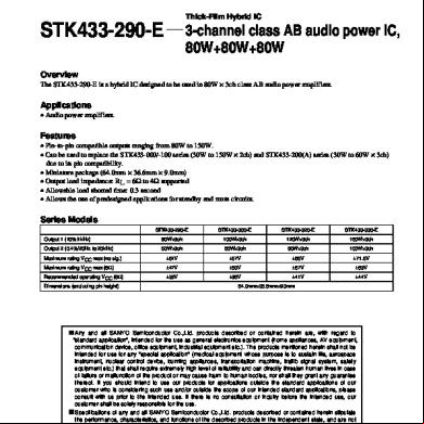
Datasheet 2p235m
October 2022 0