Transition And Diffusion Capacitance 3h1y6m
This document was ed by and they confirmed that they have the permission to share it. If you are author or own the copyright of this book, please report to us by using this report form. Report 2z6p3t
Overview 5o1f4z
& View Transition And Diffusion Capacitance as PDF for free.
More details 6z3438
- Words: 2,551
- Pages: 15
What Is meant by Fermi level in semiconductor? Derive the expression for it. Ans. Fermi level in semiconductor can be defined as the maximum energy that an
in a semiconductor have at zero degree absolute.
Assumption is the width. of energy bands are small in comparison to forbidden energy gap between them, all levels in a band have the same energy, energies of all levels in valence band are and energies of all levels in conduction band are Now no. of in conduction band, where P ( ) represents probability of an e having energy . determined by Fermi-Dirac probability distribution function
where P(E) is probability of finding an So
Now no. of
may be
…..(1) having energy E.
in valence band,
The probability P(0) of an being found in the valence band with zero energy can be determined by putting E = 0 in (1).
So
Or
i.e. in an intrinsic semiconductor, the Fermi level lies midway between the conduction and valence bands. Q. 15. What do you mean by Fermi level ? Derive the expression for Fermi level and sketch the position of intrinsic, P-type and N-type semiconductor. Ans. Fermi level can be defined as the maximum energy that an semiconductor have at zero degree absolute. Fermi Dirac probability function
in a
where K is boltzmann constant and is the Fermi level in eV. Concentration of free (it) and of holes (P) are given as
where is the no. of in conduction band, is the no. of in the valence band, is the lowest energy in conduction band in eV and is the maximum energy of valence band in eV. The only parameter that changes with the addition of impurity is fermi level . In an intrinsic semiconductor it lies in the middle of the energy gap, indicating equal concentrations of free and holes.
When donor type impurity is added to the crystal, then at a given temperature and assuming all donor atoms, the first states in the conduction band be filled. Hence it is difficult for from valence band to bridge the energy gap by the thermal generation. No. of hole pairs thermally generated are reduced. EF must be more closer to conduction band to indicate that many of energy states in that band are filled by donor and fewer holes exist in valence band. This is the position for fermi level in N-type semiconductor. Similarly must move down from the centre of the forbidden gap closer to the valence band for a P-type extrinsic semiconductor. Explain drift and diffusion of charge carriers in semiconductors. Derive an expression for the e current due to drift and diffusion. Ans. When a steady electric field E volt/metre is applied to a metal, the move to the positive terminal of The applied voltage In their way, they continuously collide with the atoms and rebound in random fashion After the collision, are accelerated and gain certain component of velocity in the direction opposite to that of applied electric field and lose their energy at the next collision. Thus the applied electric field does not stop collisions and random motion but makes the drift towards the positive terminal. The gain average drift velocity v in the direction opposite to that of applied electric field. Where, = drift velocity, mobility (av. particle drift velocity per unit electric field) and E is expressed in
.
This steady flow of in one direction caused by the applied electric field constitutes an electric current called drift current. Current density, Where as
is the conductivity of the medium in
and is given
:. The conductivity of of the semiconductor due to in conductidn band is given by where n is the no. of per unit volume of the conductor, e is the charge and is the electron mobility. Similarly, the conductivity , due to holes. where p is the number of holes per unit volume and , is hole mobility. Since in semiconductors, the conduction is by free and holes, so total conductivity is given as
In intrinsic semiconductor n = p = conductivity
, so intrinsic semiconductor
E is applied electric field, V is applied potential difference across the two ends of the conductor and ‘a’ is cross-sectional area of the conductor. In case of N-type semiconductor hole concentration is negligible and e concentration So conductivity of N-type semiconductor
similarly for P-type semiconductor Total current density due to drift of and holes on application of electric field E, J = Current density due to hole + Current density due to
The carrier currents are also due to concentration gradients in the doped material which leads to diffusion of carriers from high concentration to low concentration region. When a concentration gradient of carriers exists in a material, the charge carriers tend to move from tile region of higher concentration to the region of lower concentration. The process is called diffusion and the current due to this process is called diffusion current. The current density due to diffusion of holes is given as
where = diffusion constant = is mean free path at a reference plane x and between collisions. Similarly current density due to diffusion of is
is mean free-time
Total current in semiconductor in the sum of drift and diffusion current due to potential gradient and due to charge carrier concentration gradient respectively.
Differentiate between transition and diffusion capacitance of a p-n junction diode. Ans. Transition and Diffusion Capacitance: In reverse biased condition, due to change with respect to voltage there exists a capacitive effect called as transition capacitance denoted as CT. It is given by where, W = width of the carrier. W is related to barrier potential VB by the relation, barrier potential,
ε0 and εr are the permittivity and relative permittivity respectively. Hence, ,while
On the other hand, in forward biased condition also there exists a capacitive effect called as diffusion capacitance denoted as CD. Electronic devices are inherently sensitive to very high frequencies. in p-n diode, there are two capacitive effects present. Both types of capacitances are present in forward bias and reverse bias regions but in reverse region transition or depletion region capacitance
and
in
forward
bias
region
diffusion
capacitance is considered. Transition or space-charge capacitance : When p-n junction is in reverse bias, depletion region acts like an insulator or dielectric material while the p and n-type regions on either side have low resistance and act as a plates. Thus p-n junction is considered a parallel plate capacitor. The junction capacitance or transition capacitance or depletion region capacitance and is denoted by
. where , = increase in charge due to increase in voltage dv.
Since depletion region increases with the increase in reverse bias potential the resulting transition capacitance decreases.
Diffusion (or storage) capacitance : When a p-n junction is forward biased, capacitance, which is much larger than transition capacitance, is evident. This is diffusion capacitance . For a forward bias region, the depletion region reduced and hence potential barrier reduces. Now from n-side enter p-side and holes from p-side enter nside. These charge carriers diffuse away from the junction and progressively recombine. The density of charge carriers is higher near the junction when forward biased. Thus charge is stored on both sides of the junction and decays exponentially with distance i.e. Diffusion Capacitance
, which is observed that the
amount of stored charge varies with the applied voltage as for a capacitor.
z is mean life time carrier, then a flow of charge 9 yields a diode current I given as:
Diffusion capacitance is directly proportion to forward current through the diode.
What is meant by voltage regulation of a dc power supply? Ans. In an unregulated power supply consisting of transformer, rectifier and filter, output voltage does not remain constant and may vary considerably. The change in voltage from no load to full load condition is known as voltage regulation.
When and are no load output voltage and full load output voltage respectively. The output voltage may vary due to either change in supply voltage, change in load resistance or change in temperature. A voltage regulator is connected between the filter and the load in order to provide an almost constant dc voltage at the output terminals of the regulator. With this in power supply, it is known as regulated power supply. What is a zener diode? Explain its working and draw its characteristics. Ans. Zener diode, also known as breakdown diode is a p-n junction diode specially designed for operation in the breakdown region in reverse bias condition. The diode may use either breakdown mechanism or avalanche breakdown mechanism. Si is preferred for breakdown diode because of higher operating temperature and current capability. The knee point is more sharp for Si diodes. The symbol of zener diode and its watt-ampere characteristics are given.
When the reverse bias on a diode is increased, a point is reached when the junction breakdown and a reverse current increases abruptly. The breakdown region is the knee of the reverse characteristics, so, the breakdown voltage is called zener voltage and zener current . Breakdown diode is operated over breakdown region and current is limited by an external resistance. Zener voltage, depends upon the amount of doping. A heavily doped diode will have very thin depletion layer, so will be very low. By controlling the thickness of depletion layer and doping concentration, it is possible to make the zener diode to breakdown at specified voltage. The forward characteristics of zener are same as that of ordinary p-n junction diode. In reverse bias, it does not burn out immediately. As long as current through the diode is limited by external circuit with permissible values, it does not burn out. Zener impedance (or dynamic resistance of a zener diode) is most important parameter i.e. . It is defined as the reciprocal of the slope of the zener curve.
where , are small variations in current and voltage respectively. It is usually measured just above the knee in zener region. It decrease with increase in zener current. Zener voltage may be affected by change in ambient temperature. Effect of temperature on is given in term of temperature coefficient which is defined as percentage change in nominal zener voltage for each degree centigrade of change in junction temperature i.e.
For zener diodes with breakdown voltage of less than 5V, temperature coefficient is negative. For voltages above 6V, it is positive. And between 5 to 6V, it varies from negative to positive value.
Explain zener diode as a voltage regulator. Ans. Voltage regulation is a measure of a circuit’s ability to maintain a constant output voltage even when either input voltage or load current varies. The figure shows a zener diode’s application as voltage regulator to provide a constant voltage from a source whose voltage may vary appreciably.
A resistor is necessary to limit the reverse current through the diode to safer value. The voltage source and the resistor are so selected that the diode operates in the breakdown region. The diode voltage in this region, which is also the voltage across the load is called zener voltage and the current is zener current The series resistance, absorbs the output voltage fluctuations so as to maintain voltage across the load constant. Zener diode is reverse connected across the input voltage whose variations are to be regulated. As long as voltage across the load resistor is less than , the zener diode does not conduct. The resistors and constitute a potential divider across . At an increased supply voltage , the voltage drop across load resistor and becomes greater than the zener breakdown voltage. It then operates in breakdown region. limits from exceeding its rated maximum because zener current is
The current from the power supply splits at the junction of zener diode and the load resistor . So When zener diode operates in breakdown, remains fairly constant even though flowing through it, may vary considerably. When increases; current through zener and increases. At the same time, zener diode resistance decreases and the current through diode increases more than proportionately. As a result, greater voltage drop will occur across the series resistor and the output voltage will become very close to the original value. The reverse is also true. This a zener diode can maintain two output voltage, within a fraction of a volt when the supply or input voltage may vary over a range of several volts.
The advantage of zener voltage regulator over other voltage regulators is that it is smaller, lighter, more rugged and have a longer life. But zener regulation have some drawbacks also as their efficiency is low, output voltage varies slightly due to zener impedance and output voltage is dependent upon breakdown voltage of zener. This regulation is employed when there are small variations in load current and supply voltage.
Zener Diode A Zener diode is a p-n junction operated in the reverse biased mode to take advantage of its sharply defined breakdown voltage. The Zener voltage VZ is specified at some test value of current IZT, at which the diode will exhibit some dynamic impedance
which depends upon the zener voltage of the diode and the level of zener current.
Operation: A Zener diode may be used to regulate the load voltage at the value VZ by acting as a by value to counteract line voltage or load current variations. Diodes having a breakdown voltage below about 6V rely on the true zener effect (high electric field moves electrons from bonds), while the avalanche effect is responsible for reverse current above 6 V. Zener diodes have a temperature coefficient, αZ which generally is negative for VZ below about 6 V but positive above 6V, and is expressed in per cent of V Z per °C, with the change in Zener Voltage given by the equation.
Zener Regulator: When zener diode is forward biased, it works as a diode and drop across it is 0.7 V. When it works in breakdown region, the voltage across it is constant (VZ) and the current through diode is decided by the external resistance. Thus, zener diode can be used as a voltage regulator in the configuration shown in figure. The load line of the circuit is given by: Vs = ‘sRI’ + Vz’
To operate the zener in breakdown region Vs should always be greater than VZ. Rs is used to limit the current
The Zener on state resistance produces more IR drop as the current increases. As the voltage varies from V1 to V2 the operating point shifts from Q1 to Q2, The voltage at Q1 is V1= I1 RZ + VZ and at Q2, V2 = I2 RZ + VZ Thus, change in voltage is V2 – V1 = (I2 – I1)RZ; ΔVZ = ΔIZRZ
Reference zener diodes are available with αz as low as O.0005 % °C. The ission of a small amount of mercury gas increases the current capability of a hot cathode gas filled tube. A cold cathode or glow discharge diode may be used as a DC voltage regulator in a similar manner to a zener diode.
Related Documents c2h70

Transition And Diffusion Capacitance 3h1y6m
December 2019 42
Transition Capacitance 29505g
December 2019 55
Capacitance And Dielectrics 36675y
October 2021 0
Transition, Infinity, And Ecstasy 372065
September 2021 0
Chemistry Of Transition And Inner Transition Elements+. 4v414y
March 2021 0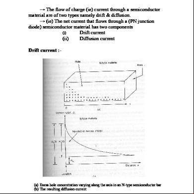
Drift And Diffusion Currents 335w27
November 2019 65More Documents from "Rishi Jha" 1c4cy
Transition And Diffusion Capacitance 3h1y6m
December 2019 42
Data Communications And Networking Questions And Answers 75u9
October 2019 293
Mriganka 5c6y60
March 2023 0
P16028 P16036 Wac Ajanta Packaging 6f5v43
October 2019 93
ccbc4005a Learner Guide 2016_v1 545e4q
July 2022 0