Cdj 200 Service Manual 3g2w5d
This document was ed by and they confirmed that they have the permission to share it. If you are author or own the copyright of this book, please report to us by using this report form. Report 2z6p3t
Overview 5o1f4z
& View Cdj 200 Service Manual as PDF for free.
More details 6z3438
- Words: 19,629
- Pages: 80
ORDER NO.
RRV3095 CDJ-200
COMPACT DISC PLAYER
CDJ-200 THIS MANUAL IS APPLICABLE TO THE FOLLOWING MODEL(S) AND TYPE(S). Model
Type
Power Requirement
CDJ-200
KUCXJ
AC120V
CDJ-200
RLTXJ
AC110-120V/AC220-240V
CDJ-200
WYXJ
AC220-240V
CDJ-200
RFXJ
AC110-120V/AC220-240V
Remarks
NECESSARY INFORMATION FOR DHHS RULES MARKED ON THE TOP COVER BELOW: CAUTION – LASER RADIATION WHEN OPEN. DO NOT STARE INTO BEAM
For details, refer to "Important Check Points for good servicing".
PIONEER CORPORATION
4-1, Meguro 1-chome, Meguro-ku, Tokyo 153-8654, Japan PIONEER ELECTRONICS (USA) INC. P.O. Box 1760, Long Beach, CA 90801-1760, U.S.A. PIONEER EUROPE NV Haven 1087, Keetberglaan 1, 9120 Melsele, Belgium PIONEER ELECTRONICS ASIACENTRE PTE. LTD. 253 Alexandra Road, #04-01, Singapore 159936
PIONEER CORPORATION 2005 T-IZY MAR. 2005 printed in Japan
1
2
3
4
SAFETY INFORMATION A
This service manual is intended for qualified service technicians ; it is not meant for the casual do-ityourselfer. Qualified technicians have the necessary test equipment and tools, and have been trained to properly and safely repair complex products such as those covered by this manual. Improperly performed repairs can adversely affect the safety and reliability of the product and may void the warranty. If you are not qualified to perform the repair of this product properly and safely, you should not risk trying to do so and refer the repair to a qualified service technician. WARNING This product contains lead in solder and certain electrical parts contain chemicals which are known to the state of California to cause cancer, birth defects or other reproductive harm. Health & Safety Code Section 25249.6 - Proposition 65
B
NOTICE (FOR CANADIAN MODEL ONLY) Fuse symbols (fast operating fuse) and/or be of identical designation.
(slow operating fuse) on PCB indicate that replacement parts must
REMARQUE (POUR MODÈLE CANADIEN SEULEMENT) Les symboles de fusible (fusible de type rapide) et/ou de remplacement doivent avoir la même désignation.
(fusible de type lent) sur CCI indiquent que les pièces
(FOR USA MODEL ONLY)
C
1. SAFETY PRECAUTIONS The following check should be performed for the continued protection of the customer and service technician.
LEAKAGE CURRENT CHECK Measure leakage current to a known earth ground (water pipe, conduit, etc.) by connecting a leakage current tester such as Simpson Model 229-2 or equivalent between the earth ground and all exposed metal parts of the appliance (input/output terminals, screwheads, metal overlays, control shaft, etc.). Plug the AC line cord of the appliance directly into a 120V AC 60 Hz outlet and turn the AC power switch on. Any current measured must not exceed 0.5 mA.
D
Reading should Leakage not be above current 0.5 mA tester
Device under test E
Test all exposed metal surfaces
Also test with plug reversed (Using AC adapter plug as required)
Earth ground
ANY MEASUREMENTS NOT WITHIN THE LIMITS OUTLINED ABOVE ARE INDICATIVE OF A POTENTIAL SHOCK HAZARD AND MUST BE CORRECTED BEFORE RETURNING THE APPLIANCE TO THE CUSTOMER.
2. PRODUCT SAFETY NOTICE Many electrical and mechanical parts in the appliance have special safety related characteristics. These are often not evident from visual inspection nor the protection afforded by them necessarily can be obtained by using replacement components rated for voltage, wattage, etc. Replacement parts which have these special safety characteristics are identified in this Service Manual. Electrical components having such features are identified by marking with a > on the schematics and on the parts list in this Service Manual. The use of a substitute replacement component which does not have the same safety characteristics as the PIONEER recommended replacement one, shown in the parts list in this Service Manual, may create shock, fire, or other hazards. Product Safety is continuously under review and new instructions are issued from time to time. For the latest information, always consult the current PIONEER Service Manual. A subscription to, or additional copies of, PIONEER Service Manual may be obtained at a nominal charge from PIONEER.
AC Leakage Test F
2
CDJ-200 1
2
3
4
5
6 IMPORTANT
7
8
LASER DIODE CHARACTERISTICS MAXIMUM OUTPUT POWER : 5 mW WAVELENGTH : 780 – 785 nm
THIS PIONEER APPARATUS CONTAINS LASER OF CLASS 1. SERVICING OPERATION OF THE APPARATUS S H O U L D B E D O N E B Y A S P E C I A L LY INSTRUCTED PERSON.
A
WARNING ! THE AEL (ACCESSIBLE EMISSION LEVEL) OF THE LASER POWER OUTPUT IS LESS THAN CLASS 1 BUT THE LASER COMPONENT IS CAPABLE OF EMITTING RADIATION EXCEEDING THE LIMIT FOR CLASS 1. A SPECIALLY INSTRUCTED PERSON SHOULD DO SERVICING OPERATION OF THE APPARATUS.
B
LABEL CHECK (for RLTXJ, WYXJ and RFXJ types) for WYXJ
for WYXJ
for RLTXJ
for RFXJ C
D
Additional Laser Caution
1. Laser Interlock Mechanism The position of the switch (S1901) for detecting loading completion is detected by the system microprocessor, and the design prevents laser diode oscillation when the switch is not in LPS1 terminal side (when the mechanism is not clamped and LPS1 signal is high level.) Thus, the interlock will no longer function if the switch is deliberately set to LPS1 terminal side. ( if LPS1 signal is low level ). In the test mode∗ the interlock mechanism will not function. Laser diode oscillation will continue, if pin 41 of TC94A15FG (IC105) on the MAIN Assy is connected to GND, or else the terminals of Q105 are shorted to each other (fault condition).
(Printed on the chassis)
E
2. When the cover is opened, close viewing of the objective lens with the naked eye will cause exposure to a Class 1 laser beam. ∗ : See page 51.
F
3
CDJ-200 5
6
7
8
1
2
3
4
[Important Check Points for Good Servicing] A
In this manual, procedures that must be performed during repairs are marked with the below symbol. Please be sure to confirm and follow these procedures.
1. Product safety Please conform to product regulations (such as safety and radiation regulations), and maintain a safe servicing environment by following the safety instructions described in this manual. 1 Use specified parts for repair. Use genuine parts. Be sure to use important parts for safety. 2 Do not perform modifications without proper instructions. Please follow the specified safety methods when modification(addition/change of parts) is required due to interferences such as radio/TV interference and foreign noise. B
3 Make sure the soldering of repaired locations is properly performed. When you solder while repairing, please be sure that there are no cold solder and other debris. Soldering should be finished with the proper quantity. (Refer to the example) 4 Make sure the screws are tightly fastened. Please be sure that all screws are fastened, and that there are no loose screws. 5 Make sure each connectors are correctly inserted. Please be sure that all connectors are inserted, and that there are no imperfect insertion. 6 Make sure the wiring cables are set to their original state. Please replace the wiring and cables to the original state after repairs. In addition, be sure that there are no pinched wires, etc.
C
7 Make sure screws and soldering scraps do not remain inside the product. Please check that neither solder debris nor screws remain inside the product. 8 There should be no semi-broken wires, scratches, melting, etc. on the coating of the power cord. Damaged power cords may lead to fire accidents, so please be sure that there are no damages. If you find a damaged power cord, please exchange it with a suitable one. 9 There should be no spark traces or similar marks on the power plug. When spark traces or similar marks are found on the power supply plug, please check the connection and advise on secure connections and suitable usage. Please exchange the power cord if necessary. D
0 Safe environment should be secured during servicing. When you perform repairs, please pay attention to static electricity, furniture, household articles, etc. in order to prevent injuries. Please pay attention to your surroundings and repair safely.
2. Adjustments To keep the original performance of the products, optimum adjustments and confirmation of characteristics within specification. Adjustments should be performed in accordance with the procedures/instructions described in this manual.
3. Lubricants, Glues, and Replacement parts Use grease and adhesives that are equal to the specified substance. Make sure the proper amount is applied.
E
4. Cleaning For parts that require cleaning, such as optical pickups, tape deck heads, lenses and mirrors used in projection monitors, proper cleaning should be performed to restore their performances.
5. Shipping mode and Shipping screws To protect products from damages or failures during transit, the shipping mode should be set or the shipping screws should be installed before shipment. Please be sure to follow this method especially if it is specified in this manual. F
4
CDJ-200 1
2
3
4
5
6
7
8
CONTENTS 1. SPECIFICATIONS .............................................................................................................................................6 2. EXPLODED VIEWS AND PARTS LIST.............................................................................................................8 2.1 PACKING SECTION ...................................................................................................................................8 2.2 EXTERIOR SECTION ..............................................................................................................................10 2.3 CONTROL SECTION...................................................................................................................12 2.4 SLOT-IN MECHANISM SECTION ............................................................................................................14 3. BLOCK DIAGRAM AND SCHEMATIC DIAGRAM ..........................................................................................16 3.1 BLOCK DIAGRAM....................................................................................................................................16 3.2 OVERALL WIRING DIAGRAM .................................................................................................................18 3.3 MAIN ASSY (1/2)......................................................................................................................................20 3.4 MAIN ASSY (2/2)......................................................................................................................................22 3.5 RLYB ASSY ..............................................................................................................................................23 3.6 DISP, KSWB, INDB, SLDB, JLED and JOGB ASSYS ..............................................................................24 3.7 JACK ASSY ..............................................................................................................................................26 3.8 ACIN, TRNS, SLMB, SECB and REGB ASSYS .......................................................................................28 3.9 VOLTAGES................................................................................................................................................30 3.10 WAVEFORMS.........................................................................................................................................32 4. PCB CONNECTION DIAGRAM ......................................................................................................................34 4.1 JACK ASSY ..............................................................................................................................................35 4.2 MAIN and RLYB ASSYS...........................................................................................................................36 4.3 DISP, KSWB, INDB, SLDB, JLED and JOGB ASSYS ..............................................................................38 4.4 ACIN, TRNS, SLMB, SECB and REGB ASSYS .......................................................................................42 5. PCB PARTS LIST ............................................................................................................................................46 6. ADJUSTMENT ................................................................................................................................................50 7. GENERAL INFORMATION .............................................................................................................................51 7.1 DIAGNOSIS..............................................................................................................................................51 7.1.1 SERVICE MODE ................................................................................................................................51 7.1.2 POWER ON SEQUENCE ..................................................................................................................58 7.1.3 DISASSEMBLY ..................................................................................................................................59 7.2 PARTS ......................................................................................................................................................64 7.2.1 IC........................................................................................................................................................64 7.2.2 FL .......................................................................................................................................................76 8. FACILITIES .........................................................................................................................................77
A
B
C
D
E
F
5
CDJ-200 5
6
7
8
1
2
3
4
1. SPECIFICATIONS A
B
• KUCXJ type 1. General
• RLTXJ, RFXJ types 1. General
System..............................Compact disc digital audio system Power requirements.....................................AC 120 V, 60 Hz Power consumption.......................................................14 W Operating temperature............+5˚C – +35˚C (+41˚F – +95˚F) Operating humidity...............................................5 % – 85 % (There should be no condensation of moisture.) Weight..............................................................3.2 kg (7.1 lb) Dimensions.........................216 (W) × 292 (D) × 99.5 (H) mm 8 – 1/2 (W) × 11 –1/2 (D) × 3 – 15/16 (H) in
System........................... Compact disc digital audio system Power requirements .... AC 110-120 V/220-240 V, 50/60 Hz Power consumption ..................................................... 16 W For Taiwan: 17 W Operating temperature .................................. +5°C – +35°C Operating humidity ........................................... 5 % – 85 % (There should be no condensation of moisture.) Weight ........................................................................3.2 kg Dimensions ...................... 216 (W) x 292 (D) x 99.5 (H) mm
2. Audio section
2. Audio section
Frequency response........................................4 Hz – 20 kHz Signal-to-noise ratio..........................110 dB or more (JEITA) Distortion.................................................... .0.006 % (JEITA)
3. Accessories
3. Accessories • Operating instructions........................................................1 • Power cord........................................................................ 1 • Audio cable....................................................................... 1 • Control cable..................................................................... 1 • Forced eject pin (housed in a groove in the bottom )... 1 • Limited warranty................................................................ 1 C
NOTE: Specifications and design are subject to possible modification with-out notice.
• Operating instructions ..................................................... • Power cord ...................................................................... • Audio cable ..................................................................... • Control cable ................................................................... • Forced eject pin (housed in a groove in the bottom )... NOTE: Specifications and design are subject to possible modification with-out notice.
System.......................... Compact disc digital audio system Power requirements .................... AC 220-240 V, 50/60 Hz Power consumption ..................................................... 16 W Operating temperature .................................. +5°C – +35°C Operating humidity ............................................ 5 % – 85 % (There should be no condensation of moisture.) Weight ....................................................................... 3.2 kg Dimensions ..................... 216 (W) x 292 (D) x 99.5 (H) mm
• You can find the voltage selector switch on the bottom plate of the unit. The factory setting for the voltage selector is 220 – 240 V. Please set it to the correct voltage for your country or region. • For Taiwan, please set to 110 – 120 V before using. Before changing the voltage, disconnect the AC power cord. Use a medium size screwdriver to change the voltage selector switch. 220-240V
2. Audio section Frequency response...................................... 4 Hz – 20 kHz Signal-to-noise ratio ....................... 110 dB or more (JEITA) Distortion ................................................... 0.006 % (JEITA)
110-120V
3. Accessories E
• Operating instructions ..................................................... • Power cord ...................................................................... • Audio cable ..................................................................... • Control cable ................................................................... • Forced eject pin (housed in a groove in the bottom )...
1 1 1 1 1
NOTE: Specifications and design are subject to possible modification with-out notice.
F
6
CDJ-200 1
2
1 1 1 1 1
Voltage selector (RLTXJ, RFXJ types only)
• WYXJ type 1. General
D
Frequency response...................................... 4 Hz – 20 kHz Signal-to-noise ratio ....................... 110 dB or more (JEITA) Distortion ................................................... 0.006 % (JEITA)
3
4
5
6
7
8
Accessories Power cord (KUCXJ : ADG7021) (RLTXJ : ADG1154) (WYXJ : ADG1154) (RFXJ : ADG7097)
Audio cable (VDE1064 or XDE3045) L= 1.5m
Control cable (ADE7108 or XDE3063) L= 1 m
A
Forced eject pin (housed in a groove in the bottom ) (DEX1008)
B
C
D
E
F
7
CDJ-200 5
6
7
8
1
2
3
4
2. EXPLODED VIEWS AND PARTS LIST NOTES: A
Parts marked by "NSP" are generally unavailable because they are not in our Master Spare Parts List. The mark found on some component parts indicates the importance of the safety factor of the part. Therefore, when replacing, be sure to use parts of identical designation. Screws adjacent to mark on product are used for disassembly. For the applying amount of lubricants or glue, follow the instructions in this manual. (In the case of no amount instructions, apply as you think it appropriate.)
2.1 PACKING SECTION
10 B
3
2
1
12
C
7
6 KUCXJ Only
8
9 5 D
4
E
11
F
13
8
CDJ-200 1
2
3
4
5
6
7
8
(1) PACKING SECTION PARTS LIST Mark No. >
1 2 3 4 5
Description
Part No.
Power Cord Audio Cable Control Cable Forced Eject Pin Operating Instructions
See Contrast table (2) VDE1064 or XDE3045 ADE7108 or XDE3063 DEX1008 See Contrast table (2) See Contrast table (2) DRM1262 AHG7117
9
Limited Warranty Seat Polyethylene Bag (0.06 x 230 x 340) Packing Sheet
10 11 12 13
Pad A Pad B Pad C Packing Case
DHA1638 DHA1639 DHA1640 See Contrast table (2)
NSP 6 NSP 7 NSP 8
A
AHG7015 B
(2) CONTRAST TABLE CDJ-200/KUCXJ, RLTXJ, WYXJ and RFXJ are constructed the same except for the following: Mark No. > NSP
1 5 6 13
Symbol and Description Power Cord Operating Instructions Limited Warranty Packing Case
C
CDJ-200/ KUCXJ
CDJ-200/ RLTXJ
CDJ-200/ WYXJ
CDJ-200/ RFXJ
ADG7021 DRB1377 ARY7043 DHG2495
ADG1154 DRB1378 Not used DHG2496
ADG1154 DRB1376 Not used DHG2494
ADG7097 DRB1378 Not used DHG2500
D
E
F
9
CDJ-200 5
6
7
8
1
2
3
4
2.2 EXTERIOR SECTION Refer to "2.3 CONTROL SECTION".
23 A K
18
40
40 43
A J
1
32 C
B
36
I
25
21
M
35
L
34
40
RLTXJ, RFXJ Only
WYXJ Only 40
K
41
41
39
32
10
I
G J
5
K
38 B
C
3 14
22
N
20 9
31
H
8
40
17
15
41
41
F F
29 27
41 4
28
6
41 33
40 41
G
J
37 41
41
16
L
D
I
11
27 D
29
42
H
E
41
29 24
A
27 L
B
M
41
41 E
M D
13
E
29
27
F
SIDE
NON- SIDE
Refer to "2.4 SLOT-IN MECHANISM SECTION".
30 41
B
7
C
2 12
A
19
41 26
19
10
41
CDJ-200 1
2
3
4
41
5
6
7
8
(1) EXTERIOR SECTION PARTS LIST Mark No.
> >
Description
Mark No.
Part No.
1 2 3 4 5
MAIN Assy RLYB Assy JACK Assy ACIN Assy TRNS Assy
DWG1587 DWX2429 DWX2433 See Contrast table (2) See Contrast table (2)
6 7 8 9 10
SLMB Assy SECB Assy REGB Assy Fuse (FU11) Power Transformer (T22)
DWS1355 DWR1394 DWR1393 See Contrast table (2) See Contrast table (2)
11 12 13 14 15
24P Flexible Cable 32P Flexible Cable 24P Flexible Cable 9P Flexible Cable Earth Lead Unit/300V
DDD1275 DDD1276 DDD1278 DDD1279 DDF1032
Connector Assy Power Button Silicone Sheet D5 L Insulator Protector
PF03PP-B17 DAC2254 DEB1456 DEC2250 DEC2808
PU Caution PCB Stay
DEC2856 DNH2640
16 17 NSP 18 19 20 21 22
23 24 25
Description
Part No.
Heatsink Trans. Plate Card Spacer
DNH2641 DNH2670 DNK2769
Chassis Damper Earth Spring Float Spring G5 FPC Guard
See Contrast table (2) CNV6011 DBH1398 DBH1494 DBK1282
31 32 33 34 35
Mecha Plate Nyron Rivet (3 x 4.5) Cord Clamper Caution Label HE Caution Label
DNH2642 RBM-003 RNH-184 See Contrast table (2) See Contrast table (2)
36 37 38 39 40
Caution Label Nut M12 DM Screw Screw Screw
See Contrast table (2) DBN1012 DBA1260 BBZ40P060FTC BBZ30P060FTC
41 42 43
Screw Jumper Wire 6P(J904) 15P Flexible Cable
BPZ30P080FTC D20PDY0610E DDD1277
NSP 26 27 28 29 30
A
B
C
(2) CONTRAST TABLE CDJ-200/KUCXJ, RLTXJ, WYXJ and RFXJ are constructed the same except for the following: CDJ-200/ KUCXJ
CDJ-200/ RLTXJ
CDJ-200/ WYXJ
CDJ-200/ RFXJ
DWR1388 DWR1391 REK1111
DWR1389 DWR1392 Not used
DWR1387 DWR1391 Not used
DWR1389 DWR1392
>
4 ACIN Assy 5 TRNS Assy 9 Fuse (FU11 : 2.0A/125V)
>
9 Fuse (FU11 : T1AL250V)
Not used
REK1022
REK1022
REK1022
>
10 Power Transformer (T22)
DTT1172
DTT1171
DTT1171
DTT1171
NSP
26 34 35 36
DNK4423 Not used Not used Not used
DNK4424 Not used Not used PRW1018
DNK4386 PRW1233 VRW1094 Not used
DNK4427 Not used Not used DRW2248
Mark No.
Symbol and Description
Chassis Caution Label HE Caution Label Caution Label
D
Not used
E
F
11
CDJ-200 5
6
7
8
1
2
3
4
2.3 CONTROL SECTION 21
A
Dyefree GEM1036 (ZLX-ME413A)
22
23
27
B
34
34
20
5
28
G 33 D 16
35 C
19
18
D
9
E
8
34 25
A
26 15
3
13
B
24
D
10
A
2
12 30
36
E
C
H 34
SIDE
NON- SIDE
29
31
B
E
C
6
34
7
F
F
14
11
34
34 4
To MAIN CN105
C D 37
1 38
34
34
17
E
34
12
34
CDJ-200 1
2
3
4
5
6
7
8
CONTROL SECTION PARTS LIST Mark No.
Description
Part No.
1 2 3 4 5
DISP Assy KSWB Assy INDB Assy SLDB Assy JLED Assy
DWG1588 DWS1356 DWX2438 DWX2430 DWX2432
6 7 8 9 10
JOGB Assy 15P Flexible Cable PLAY Button SEARCH Button LOOP Button
DWX2431 DDD1277 DAC2244 DAC2245 DAC2246
11 12 13 14 15
RELOOP Button BEAT LOOP Button TIME Button EJECT Button JET Button
DAC2270 DAC2271 DAC2249 DAC2253 DAC2266
16 17 18 19 20
Slide Sheet (GRAY) Earth Plate Vessel Sheet Control A Control B
DAH2374 DBK1224 DEC2751 DNK4384 DNK4385
21 22 23 24 25
Jog Dial POM Ring Jog Lens Front Lens Reflector
DNK4387 DNK4388 DNK4389 DNK4390 DNK4391
26 27 28 29 30
BEAT Lens Display Slide Knob (SILVER) TEMPO Button Assy TEMPO Button
DNK4392 DNK4492 DNK4448 DXA2014 DAC2258
31 32 33 34 35
TEMPO Lens ••••• Nut M9 Screw JOG Washer
DNK4421
36 37 38
Jumper Wire 3P Jumper Wire 4P Jumper Wire 6P
D20PDY0305E D20PDY0405E D20PDY0610E
A
B
C
D
DBN1008 BPZ30P080FTC DBF1002
E
F
13
CDJ-200 5
6
7
8
1
2
3
4
2.4 SLOT-IN MECHANISM SECTION Grease GYA1001 (ZLB-PN397B)
A
1
11
20 21 Dyefree GEM1036 (ZLX-ME413A) 9
23 10
18 17 Grease GYA1001 (ZLB-PN397B)
7
B
22
24
13
14
19 C
Dyefree GEM1036 (ZLX-ME413A)
8
Dyefree GEM1036 (ZLX-ME413A)
15
Cleaning liquid : GEM1004 Cleaning paper : GED-008
25
To RLYB CN12 (Pickup)
16
3
4 5 To RLYB CN16 (Loading Motor)
12
D
25 To RLYB CN14 (Stepping Motor)
25
Grease GYA1001 (ZLB-PN397B)
6
27 2
25
31
Note: The TM. Assy 03-S is supplied only in assembly form, not as a single part.
E
To MAIN CN102 (Spindle Motor)
26
28 F
30
14
CDJ-200 1
2
3
4
SIDE
29
NON- SIDE
30
5
6
7
8
SLOT-IN MECHANISM SECTION PARTS LIST Mark No.
Description
Part No.
NSP 1 2 3 NSP 4 NSP 5
Slot-in Mecha SV Assy TM. Assy 03-S DC Motor Assy-S Worm Gear DC Motor S (ROHS)
DXA2005 VXX2909 DXX2510 DNK3910 DXM1230
6 7 8 9 10
Connector Assy Clamp Spring Guide Spring SW Lever Spacer SV Loading Lever
PF02PY-B22 DBH1374 DBH1375 DEC2831 DNK3406
11 12 13 14 15
Main Cam Disc Guide Clamp Arm Eject Lever Lever AP
DNK3407 DNK3478 DNK3576 DNK3684 DNK3835
16 17 18 19 20
Lever BP Loading Gear Drive Gear Loading Base SV SW Lever SV1
DNK3836 DNK3911 DNK3912 DNK4369 DNK4370
21 22 23 24 25
SW Lever SV2 Gear Holder SV Clamper 04 Assy Screw Floating Rubber (SI)
DNK4371 DNK4372 DXB1859 BPZ20P060FTC VEB1351
26 27 28 29 30
Float Base 04 Assy Spacer POR (T3) Vessel Cushion A Vessel Cushion B Vessel Cushion C
DXB1838 DEB1566 DEC2852 DEC2853 DEC2854
31
Front Sheet
DED1132
A
B
C
D
E
F
15
CDJ-200 5
6
7
8
1
2
3
4
3. BLOCK DIAGRAM AND SCHEMATIC DIAGRAM 3.1 BLOCK DIAGRAM A
TM. ASSY 03-S (VXX2909) SPINDLE MOTOR 04
STEPPING MOTOR 04
B PICKUP ASSY
DC MOTOR ASSY-S (DXX2510)
C
L SLMB ASSY
COMPARATOR
B
RLYB ASSY
D
N
REGB ASSY
DIGITAL OUT
CONTROL
E
For KUCXJ, WYXJ
M SECB ASSY
J
ACIN ASSY
J2
K For RLTXJ, RFXJ
TRNS ASSY
S2 BROWN
S1
VIOLET
F
J3
BLUE
J
ACIN ASSY
16
CDJ-200 1
2
3
4
5
6
7
8
A
A
MAIN ASSY
B
PHONES
C
AUDIO OUT
I
JACK ASSY
D
D
E
KSWB ASSY
F C
E
INDB ASSY
SLDB ASSY
DISP ASSY
F
H
G
JOGB ASSY
JLED ASSY 17
CDJ-200 5
6
7
8
1
2
3
4
3.2 OVERALL WIRING DIAGRAM A
3
SPINDLE MOTOR 04
TM. ASSY 03-S (VXX2909)
SLOT-IN MECHA SV ASSY (DXA2005)
B
1 2 4 5 6 7 8 9 10 11 12
(S) (S) (S) (S)
STEPPING MOTOR 04
(F) (F) (T) (T)
B RLYB ASSY (DWX2429)
(RF) (RF) (T)
PICKUP ASSY
C
(T) (RF) (RF)
DC MOTOR ASSY-S (DXX2510) D
L FOR KUCXJ, WYXJ POWER CORD KUCXJ : ADG7021 WYXJ : ADG1154
SLMB ASSY (DWS1355)
J
ACIN ASSY (KUCXJ : DWR1388) (WYXJ : DWR1387)
K TRNS ASSY (KUCXJ, WYXJ : DWR1391) (RLTXJ, RFXJ : DWR1392)
KUCXJ : XKP3042 WYXJ : XKP3041
POWER CORD RLTXJ : ADG1154 RFXJ : ADG7097
J ACIN ASSY (RLTXJ, RFXJ : DWR1389)
FOR RLTXJ, RFXJ (RF) (T)
F
: RF DATA SIGNAL ROUTE
ASSY N REGB (DWR1393)
E
ASSY M SECB (DWR1394)
: TRACKING DATA SIGNAL ROUTE
(F)
: FOCUS SERVO LOOP LINE : TRACKING SERVO LOOP LINE (S) : STEPPING SERVO LOOP LINE (T)
18
CDJ-200 1
2
3
4
5
6
7
8
A
D
E INDB ASSY (DWX2438)
C
A A 1/2, A 2/2
F
ASSY H JOGB (DWX2431)
DISP ASSY (DWG1588)
MAIN ASSY (DWG1587)
B
ASSY G JLED (DWX2432)
KSWB ASSY (DWS1356)
C
SLDB ASSY (DWX2430)
D
L AUDIO OUT
I
R
JACK ASSY (DWX2433)
E PHONES
÷ When ordering service parts, be sure to refer to "EXPLODED VIEWS and PARTS LIST" or "PCB PARTS LIST". ÷ The > mark found on some component parts indicates the importance of the safety factor of the part. Therefore, when replacing, be sure to use parts of identical designation. ÷ : The power supply is shown with the marked box. 19
CDJ-200 5
6
F
7
8
1
2
3
4
3.3 MAIN ASSY (1/2)
A 1/2 MAIN ASSY (DWG1587)
C
CN501
A
B
UPDATE CONNECTOR
(D)
(D)
(D)
(D)
C
(D)
D
A 2/2
E
A 2/2 CAUTION : FOR CONTINUED PROTECTION AGAINST RISK OF FIRE. REPLACE ONLY WITH SAME TYPE NO. DEK1092- 466.200 MFD, BY LITTELFUSE INK. FOR IC123. (RF) (T)
F
: RF DATA SIGNAL ROUTE
(D)
: TRACKING DATA SIGNAL ROUTE
: AUDIO DATA SIGNAL ROUTE
(F)
: FOCUS SERVO LOOP LINE (T) : TRACKING SERVO LOOP LINE (S) : STEPPING SERVO LOOP LINE
A 1/2 20
: AUDIO SIGNAL ROUTE (L ch) : AUDIO SIGNAL ROUTE (Digital)
CDJ-200 1
2
3
4
5
6
I
7
8
M CN905
CN701
A
2
1
(RF) (RF)
(RF)
(T)
(T)
(RF)
B
(S) (S) (S) (S)
9
7
6
12
8
C
5 3
13
4 (F)
10
(F) (T) (T)
(D)
14
(RF) (RF) (T)
(F)
(T) (F)
(RF) (T)
D (T) (RF)
(S) (S)
(S) (S)
B
CN11
(S) (S) (S) (S)
E
11 (F)
15 16
(F) (T)
(T)
To SPINDLE MOTOR 04
F
A 1/2 21
CDJ-200 5
6
7
8
1
2
3
4
3
4
3.4 MAIN ASSY (2/2) A
A 2/2 MAIN ASSY (DWG1587)
B
C
A 2/2 A 2/2
D
E
F
A 2/2 22
CDJ-200 1
2
5
6
7
8
3.5 RLYB ASSY (RF) (T)
: RF DATA SIGNAL ROUTE : TRACKING DATA SIGNAL ROUTE
A
(F)
: FOCUS SERVO LOOP LINE (T) : TRACKING SERVO LOOP LINE (S) : STEPPING SERVO LOOP LINE
B RLYB ASSY (DWX2429) (S) (S) (S) (S)
(S) (S) (S) (S)
To STEPPING MOTOR 04
To DC MOTOR ASSY-S
(S)
L
(S)
B
CN1901
(S) (S)
A 1/2 CN101
C
(F)
(F)
(F)
(F) (T)
(T)
(T)
(T)
(RF)
(RF) (RF) (T)
(RF) (T)
(T)
(T)
(RF) (RF)
(RF) (RF)
D
(T) (T) (F) (F)
(T) (T) (RF) (RF)
E
To PICKUP ASSY CN1
(T) (T) (F)
F
(F)
B 23
CDJ-200 5
6
7
8
1
2
3
4
3.6 DISP, KSWB, INDB, SLDB, JLED and JOGB ASSYS
D KSWB ASSY (DWS1356)
C DISP ASSY (DWG1588)
INDB ASSY (DWX2438)
A
E
B
C
D
E
F
SLDB ASSY (DWX2430)
F
C D E F 24
CDJ-200 1
2
3
4
5
6
7
8
DISP ASSY S501 : EJECT (0) S502 : TEMPO ±6/±10/±16 S503 : MASTER TEMPO S504 : TEXT MODE S505 : TIME MODE S506 : AUTO CUE S507 : BEAT LOOP LOOP S508 : RELOOP/EXIT S509 : JET S510 : WAH DIGITAL JOG BREAK S511 : ZIP S512 : HOLD/RESET S513 : OUT/OUT ADJUST S514 : IN/REAL TIME CUE/HOT LOOP
KSWB ASSY S601 : PLAY/PAUSE (6) S602 : CUE S603 : ¡ SEARCH S604 : 1 S605 : ¢ TRACK SEARCH S606 : 4 S607 : = FOLDER SEARCH S608 : + JOGB ASSY S600 : JOG (–REV
A
FWD+)
B
A 1/2 CN105
C
D
H JOGB ASSY (DWX2431)
E
F
G JLED ASSY (DWX2432)
C G H 25
CDJ-200 5
6
7
8
1
2
3
4
3
4
3.7 JACK ASSY A
I
JACK ASSY (DWX2433)
B
A 1/2 CN104
C
D
E
F
I 26
CDJ-200 1
2
5
6
7
8
A : AUDIO SIGNAL ROUTE (L ch)
B
L AUDIO OUT R
C
D
PHONES
E
F
I 27
CDJ-200 5
6
7
8
1
2
3
4
3.8 ACIN, TRNS, SLMB, SECB and REGB ASSYS A
• NOTE FOR FUSE REPLACEMENT CAUTION - FOR CONTINUED PROTECTION AGAINST RISK OF FIRE. REPLACE WITH SAME TYPE AND RATINGS ONLY.
ASSY K TRNS (KUCXJ, WYXJ : DWR1391) (RLTXJ, RFXJ : DWR1392)
FOR RLTXJ, RFXJ
J
B
ACIN ASSY (RLTXJ, RFXJ : DWR1389) T22 POWER TRANSFORMER : DTT1171
S1 : POWER (ON/OFF) S2 : VOLTAGE SELECTOR
FU11 : REK1022 (T1AL250V)
C
FU11 KUCXJ : REK1111 (2.0A/125V) WYXJ : REK1022 (T1AL250V)
S1 : POWER (ON/OFF) T22 POWER TRANSFORMER KUCXJ : DTT1172 WYXJ : DTT1171
KUCXJ : XKP3042 WYXJ : XKP3041
D
J
ACIN ASSY (KUCXJ : DWR1388) (WYXJ : DWR1387)
FOR KUCXJ, WYXJ
E
B
CN15
L
SLMB ASSY (DWS1355)
F
J K L 28
CDJ-200 1
2
3
4
5
6
7
8
A : AUDIO SIGNAL ROUTE (Digital)
M SECB ASSY (DWR1394) N
B
REGB ASSY (DWR1393)
A 1/2 CN103
C
D
CONTROL
E
DIGITAL OUT
F
K M N 29
CDJ-200 5
6
7
8
1
2
3
4
3.9 VOLTAGES A A
MAIN ASSY IC105 (TC94A15FG-K)
IC101 (NJM2374AD) Pin Voltage (V) 1 7.92 2 3.56 3 0.873 4 -0.01 5 1.218 6 8.01 7 7.95 8 7.93 IC102 (NJM2374AM-TFB)
B
Pin Voltage (V) 1 7.11 2 0.389 3 -6.00 4 -6.76 5 -5.56 6 7.13 7 7.11 8 7.11 IC104 (PQ1M335M2SPQ-TRB)
C
Pin Voltage (V) 1 1.21 2 0 3 5 4 5 5 3.29 IC106 (NJU7016M-TFB) Pin Voltage (V) 1 174.2m 2 166.4m 3 169.7m 4 0 5 1.667 6 1.979 7 1.642 8 3.23
D
IC108 (NJU7016M-TFB) Pin Voltage (V) 1 1.617 2 1.617 3 1.617 4 0.01 5 1.617 6 1.678 7 1.678 8 3.34 IC109 (BH2220FVM-TLB)
E
Pin Voltage (V) 1 2.23 2 1.110 3 0.2m 4 3.24 5 0 6 71.2m 7 64.3m 8 102.2m IC110 (NJM2880U1-05-TLB)
F
Pin Voltage (V) 1 7.13 2 0 3 1.262 4 5 5 7.13
IC107 (BD7907FS-TBB)
IC117 (K4S641632H-TC75-K)
Pin Voltage (V) 1 2.41 2 2.41 3 2.40 4 2.40 5 2.39 6 2.39 7 0.532 8 0 9 0.682 10 7.23 11 0.678 12 0 13 0 14 0 15 0 16 0 17 0 18 0.682 19 7.23 20 7.23 21 1.624 22 2.2m 23 3.2 24 1.675 25 0 26 1.642 27 1.616 28 1.896 29 0.909 30 7.23 31 7.23 32 7.13 33 0 34 6.74 35 6.50 36 3.80 37 3.43 38 0 39 0 40 0 41 0 42 0 43 0 44 7.23 45 3.50 46 3.71 47 3.59 48 3.63 49 3.25 50 3.25 51 7.23 52 1.612 53 1.641 54 4.80
Pin Voltage (V) 1 3.23 2 0.32 3 3.25 4 0.227 5 0.206 6 0 7 0.185 8 0.206 9 3.25 10 0.208 11 0.206 12 0.198 13 0.211 14 3.25 15 0.18m 16 3.25 17 3.24 18 3.24 19 3.24 20 1.0m 21 1.0m 22 2.0m 23 3.25 24 3.25 25 3.25 26 1.8m 27 3.25 28 0 29 3.26 30 1.0m 31 3.26 32 1.2m 33 3.26 34 1.2m 35 2.0m 36 0 37 3.26 38 1.634 39 1.0m 40 0 41 0 42 0.335 43 3.23 44 0.399 45 0.530 46 0 47 0.305 48 0.489 49 3.23 50 0.574 51 0.301 52 0 53 0.495 54 0
IC114 (NJM2903M-TLB)
IC121 (MM1561JF-TFB)
Pin Voltage (V) 1 1.521 2 1.638 3 1.638 4 0 5 1.832 6 1.678 7 1.722 8 3.23 IC115 (M51957BFP-TFB)
Pin Voltage (V) 1 1.823 2 1.395 3 0 4 0.540 5 3.34 6 0 7 3.33
Pin Voltage (V) Pin Voltage (V) 1 0.15 51 1.630 2 3.06 52 0 3 185.3m 53 2.42 4 3.29 54 1.617 5 0.01m 55 1.603 6 2.94 56 1.797 7 1.097 57 1.633 8 35.5m 58 1.636 9 20.5m 59 3.29 10 0 60 1.697 11 3.29 61 1.635 12 1.807 62 1.638 13 3.29 63 1.612 14 1.642 64 1.669 15 1.621 65 0 16 0.488 66 0 17 1.642 67 1.86 18 1.642 68 0 19 1.638 69 0 20 0.615 70 3.3 21 1.766 71 0 22 1.627 72 0 23 1.628 73 1.509 24 0 74 1.592 25 1.656 75 3.29 26 0 76 0 27 1.635 77 1.598 28 1.680 78 3.29 29 3.3 79 1.606 30 1.463 80 1.587 31 1.638 81 0 32 1.477 82 0.04 33 1.671 83 0 34 0 84 3.24 35 1.632 85 3.20 36 1.278 86 3.19 37 1.278 87 3.19 38 3.3 88 3.18 39 0.521 89 3.05 40 3.28 90 3.25 41 2.19 91 3.29 42 174.3m 92 1.819 43 0 93 3.29 44 1.728 94 0 45 1.720 95 3.28 46 1.710 96 3.28 47 1.726 97 1.681 48 1.730 98 1.715 49 1.737 99 1.648 50 0.190 100 0 IC112 IC111 (TC7WU04FU-TRB) (PCM1742KE-TRB) Pin Voltage (V) 1 1.708 2 1.715 3 1.769 4 0 5 1.727 6 1.727 7 1.759 8 3.33 IC113 (TC7WU04FU-TRB) Pin Voltage (V) 1 1.628 2 1.628 3 1.609 4 0 5 1.678 6 1.678 7 1.722 8 3.23
Pin Voltage (V) 1 1.668 2 0.02m 3 1.666 4 0 5 3.33 6 5.01 7 2.52 8 2.48 9 0 10 2.49 11 2.4m 12 2.4m 13 70.8m 14 64.2m 15 3.23 16 1.489
Pin Voltage (V) 1 0 2 1.372 3 1.372 4 0 5 1.229 6 3.33 7 3.33 8 0
30
IC119 IC118 (MBM29LV800TE90PFTN-K) (DSPD56367PV150) Pin Voltage (V) 1 2.64 2 2.60 3 0.881 4 2.44 5 0.881 6 2.16 7 1.307 8 2.25 9 0 10 0 11 2.83 12 3.23 13 0 14 -102.3 15 3.23 16 155.4m 17 0 18 2.45 19 0.894 20 2.44 21 0.928 22 2.53 23 0.719 24 2.52 25 2.1 26 3.26 27 0 28 3.26 29 0.454 30 0 31 0.312 32 0.399 33 0.713 34 0.385 35 0.552 36 0.398 37 3.24 38 0.563 39 0.585 40 0.589 41 0.721 42 0.505 43 0.294 44 0.472 45 0.458 46 0 47 3.24 48 2.14
IC122 (TC7SU04FU-TLB) Pin Voltage (V) 0 1 2 1.507 3 0 4 1.851 5 3.34
Pin Voltage (V) 1 64.1m 2 3.23 3 11.6m 4 0.556 5 0.3m 6 23.5m 7 0.2m 8 3.33 9 0 10 0.2m 11 1.545 12 1.666 13 1.683 14 1.678 15 1.663 16 1.886 17 0.3m 18 1.824 19 0 20 3.35 21 0.2m 22 0.2m 23 3.27 24 3.28 25 3.35 26 0 27 1.703 28 1.895 29 3.34 30 18.4m 31 0.2m 32 0.2m 33 0.2m 34 0.2m 35 0.2m 36 0.2m 37 0.1m 38 3.35 39 0 40 0.1m 41 0.1m 42 0 43 0.1m 44 3.18 45 1.824 46 0.441 47 0 48 0.195 49 3.35 50 0 51 0 52 0.423 53 0.193 54 0 55 1.725 56 1.824 57 3.35 58 0 59 0.346 60 0.560 61 0 62 0 63 3.35 64 3.35 65 3.35 66 0 67 0.320 68 0.511 69 0.786 70 0.685 71 0 72 0.754
Pin Voltage (V) 73 0.636 74 3.35 75 0 76 0.512 77 0.221 78 0.305 79 0.439 80 3.35 81 0 82 0.502 83 0.384 84 0.325 85 0.348 86 3.35 87 0 88 0.413 89 0.396 90 0 91 3.35 92 0.361 93 0.389 94 0.200 95 3.35 96 0 97 0.739 98 0.242 99 0.378 100 1.6m 101 1.6m 102 1.7m 103 3.35 104 0 105 1.7m 106 1.7m 107 1.7m 108 1.7m 109 1.7m 110 1.7m 111 3.35 112 0 113 1.6m 114 1.6m 115 1.6m 116 1.6m 117 1.5m 118 0 119 3.35 120 0 121 1.4m 122 1.4m 123 1.3m 124 1.3m 125 1.2m 126 3.35 127 0 128 1.2m 129 3.35 130 0 131 1.3m 132 1.3m 133 1.5m 134 0.2m 135 23.7m 136 0.3m 137 3.34 138 3.34 139 0.475 140 3.33 141 3.33 142 3.33 143 71.3m 144 3.33
CDJ-200 1
2
3
4
5
A
MAIN ASSY
IC120 (SCF5249LAG120-K) Pin Voltage (V) 1 3.3 2 3.27 3 0.443 4 2.18 5 1.326 6 2.17 7 1.149 8 2.17 9 1.685 10 3.20 11 3.27 12 3.33 13 0.347 14 0.563 15 57.4m 16 3.25 17 0.545 18 0.390 19 0.394 20 0 21 0.545 22 0.662 23 0 24 0.433 25 3.25 26 0.489 27 1.8 28 2.61 29 0 30 0 31 0.710 32 2.71 33 2.64 34 3.26 35 139.5m 36 0.581 37 0 38 1.271 39 2.2m 40 2.84 41 2.76 42 2.76 43 2.76 44 3.25 45 3.25 46 41.6m 47 18.2m 48 0.469 49 0.636 50 3.26 51 0.636 52 0.402 53 0.506 54 0.486 55 0.332 56 3.27 57 0.440 58 2.5m 59 1.3m 60 0 61 1.638 62 3.25 63 1.772 64 35.6m 65 3.35 66 1.615 67 1.662 68 3.27 69 3.27 70 1.534 71 1.660 72 0
6
C
N
DISP ASSY
IC501 (PEG083A8-K)
Pin Voltage (V) 73 0 74 3.05 75 1.648 76 3.19 77 1.63 78 1.68 79 3.25 80 3.34 81 1.659 82 0 83 1.8 84 0 85 0 86 3.28 87 0 88 1.775 89 3.19 90 1.603 91 3.21 92 3.17 93 1.547 94 0 95 3.27 96 0 97 1.775 98 2.92 99 3.34 100 0 101 0 102 0 103 0 104 0 105 0 106 3.28 107 0 108 0 109 3.34 110 0 111 0 112 3.27 113 3.3 114 0 115 1.543 116 3.26 117 3.34 118 0 119 3.33 120 3.33 121 36.0m 122 0 123 3.34 124 3.27 125 1.635 126 0.971 127 2.71 128 4.56 129 3.26 130 0 131 2.19 132 2.75 133 2.72 134 2.75 135 0 136 2.74 137 2.73 138 0.774 139 2.83 140 0.766 141 1.776 142 2.80 143 0 144 3.27
7
IC506 (PST994D-T)
Pin Voltage (V) Pin Voltage (V) 1 2.39 51 -10.61 2 7.4m 52 -19.00 3 4.78 53 -17.91 4 4.78 54 -14.04 5 4.78 55 -22.6 6 0 56 -15.73 7 4.78 57 -14.93 8 79.1m 58 -16.31 9 80.1m 59 -22.4 10 80.4m 60 -24.3 11 0.7m 61 -17.86 12 80.1m 62 -24.3 13 0 63 -26.9 14 0 64 -28.7 15 0 65 -23.2 16 4.78 66 -15.13 17 0 67 -22.5 18 4.79 68 -6.94 19 0 69 -6.50 20 0 70 -15.05 21 0 71 -20.5 22 2.39 72 -14.58 23 2.03 73 -29.7 24 4.79 74 -29.7 25 0.970 75 -29.7 26 2.38 76 -27.3 27 4.78 77 -27.5 28 4.78 78 -27.5 29 4.78 79 -25.4 30 0 80 -27.4 31 0 81 -27.4 32 0 82 -27.5 33 4.77 83 -27.5 34 4.77 84 -27.5 35 4.56 85 -27.5 36 4.00 86 -27.5 37 -26.6 87 -27.5 38 -7.25 88 -27.5 39 -5.02 89 -30.0 40 -6.25 90 4.77 41 -24.0 91 2.26 42 -8.16 92 0 43 -26.7 93 4.77 44 -26.5 94 4.78 45 -24.1 95 4.78 46 -9.80 96 4.78 47 -8.23 97 0 48 -6.55 98 4.79 49 -9.61 99 4.77 50 -13.56 100 2.29
Pin Voltage (V) 1 4.78 2 0 3 4.77
8
REGB ASSY A
IC911 (BA05T) Pin Voltage (V) 1 8 2 0 3 5 IC912 (PQ15RW11) Pin Voltage (V) 1 10.5 2 7.3 3 0 4 2.57
B
C
D
E
F
31
CDJ-200 5
6
7
8
1
2
3
4
3.10 WAVEFORMS Note : The encircled numbers denote measuring point in the schematic diagram. A
A 1/2 MAIN ASSY • at play 1
• at load-out
RFO V: 500mV/div. H: 200nsec/div.
3 4 5 6
LPS1 V: 5V/div. LPS2 V: 5V/div. LO+ V: 5V/div. LO– V: 5V/div.
• at start-up
H: 500msec/div.
7
H: 500msec/div.
9
H: 500msec/div.
10
H: 500msec/div.
11
FE V: 1V/div. TE V: 1V/div. DMO V: 1V/div. INSIDE V: 5V/div.
H: 200msec/div. H: 200msec/div. H: 200msec/div. H: 200msec/div.
B 3 7 4 9 5
10
6
C
• at play 2
11
• at focus-in
AGCRF V: 500mV/div. H: 200nsec/div.
7
• at stopped
FE V: 5V/div. H: 2msec/div.
7 9 10 12
FE V: 1V/div. TE V: 1V/div. DMO V: 1V/div. LDO V: 5V/div.
H: 100msec/div. H: 100msec/div. H: 100msec/div. H: 100msec/div.
7
D 9
10
12
• at load-in 3 4 E
5 6
LPS1 V: 5V/div. LPS2 V: 5V/div. LO+ V: 5V/div. LO– V: 5V/div.
• at focus-in
H: 200msec/div.
7
H: 200msec/div.
8
• at auto adjustment
FE V: 5V/div. H: 100msec/div. FOO V: 5V/div. H: 100msec/div.
7 8
H: 200msec/div.
9
H: 200msec/div.
13
FE V: 1V/div. FOO V: 1V/div. TE V: 1V/div. TRO V: 2V/div.
H: 200msec/div. H: 200msec/div. H: 200msec/div. H: 200msec/div.
3 7 4
7
5
8
8
F
9 6 13
32
CDJ-200 1
2
3
4
5
6
7
8
A 1/2 MAIN ASSY • at pause 9 13 1 14
TE V: 1V/div. TRO V: 2V/div. RFO V: 1V/div. SBOK V: 5V/div.
A
• at play H: 2msec/div.
9
H: 2msec/div.
13
H: 2msec/div.
15
H: 2msec/div.
16
TE V: 1V/div. H: 1sec/div. TRO V: 2V/div. H: 1sec/div. ST1 (IC109-pin 1) V: 1V/div. H: 1sec/div. ST2 (IC109-pin 2) V: 1V/div. H: 1sec/div.
B 9
9 13
13 15 1 16 14
• at scan 9 13 1 14
TE V: 1V/div. TRO V: 1V/div. RFO V: 1V/div. SBOK V: 5V/div.
• at scan H: 2msec/div.
9
H: 2msec/div.
13
H: 2msec/div.
15
H: 2msec/div.
16
9
9
13
13
C
TE V: 1V/div. H: 50msec/div. TRO V: 2V/div. H: 50msec/div. ST1 (IC109-pin 1) V: 1V/div. H: 50msec/div. ST2 (IC109-pin 2) V: 1V/div. H: 50msec/div.
D 15 1 16 14
• at track search 9 13 1 14
TE V: 1V/div. TRO V: 1V/div. RFO V: 1V/div. SBOK V: 5V/div.
• at track search
H: 50msec/div.
9
H: 50msec/div.
13
H: 50msec/div.
15
H: 50msec/div.
16
9
9
13
13
1
15
TE V: 1V/div. H: 20msec/div. TRO V: 2V/div. H: 20msec/div. ST1 (IC109-pin 1) V: 2V/div. H: 20msec/div. ST2 (IC109-pin 2) V: 2V/div. H: 20msec/div.
E
F
16 14
33
CDJ-200 5
6
7
8
1
2
3
4
4. PCB CONNECTION DIAGRAM NOTE FOR PCB DIAGRAMS : A
1. Part numbers in PCB diagrams match those in the schematic diagrams. 2. A comparison between the main parts of PCB and schematic diagrams is shown below. Symbol In PCB Diagrams
Symbol In Schematic Diagrams B C E B C E
3. The parts mounted on this PCB include all necessary parts for several destinations. For further information for respective destinations, be sure to check with the schematic diagram. 4. View point of PCB diagrams.
Part Name
Connector
Capacitor
Transistor
B C E B
C
E B
C
SIDE A
E Transistor with resistor
B C E D
B
G S D
G S Field effect transistor
D G S
P.C.Board
Chip Part
SIDE B
Resistor array
3-terminal regulator
C
D
E
F
34
CDJ-200 1
2
3
4
L703
VR701
L705 L706 C718
C717
L701
C719 L704
L707
R
D701
Q709
D702 R707
R737
R738
L
L708
C707 R709
C701
C711
C712
W180
W189
C714
JA702 W188 IC702
W199
L
8
7
DWX2433
W181
W155
C713
1 1
R713
R714
8.V+7A 9.V-7A
1.ROUT 2.GND 3.GND 4.LOUT 5.GNDH 6.GNDH 7.MUTE
W154
R
R715
R716
V+7A
GNDH
7.MUTE 8.V+7A 9.V-7A
C703
JACK DWX2433
JA701
5
4 4
JACK
C716
R722
MUTE MUTE R732 C709 R734
C710
V-7A
4.LOUT
SIDE=TOP
R723
C730 R724
R731 R726
R711
R712
2.GND R702 3.GND 5.GNDH R701 6.GNDH
C704
W178
C732
R725
R727
C731
R705
C735
C734
CN701
W175
R720
R729 R730
R703
R704 Q701 C737
R733
Q703
1.ROUT
SIDE=TOP
W186
R719
L
R
R708
C733
R710
9
Q710
C736 Q702
Q707
C708 Q704
Q708 R728
L702
R706
C700
W179
C715
W177
8 8
R721
C705
5
CN701
R 3
IC702
W176
1
R
GNDH
6
3
4
1
V+7A
6
GNDH
2
V-7A
R ch MUTE
9
5
1
IC701
1
5 C706 2
8
W174
4
JACK ASSY L
1
JACK ASSY
V-7A
ADD SOLDER
I W198
R
1
9
I
LF
5 7 8
4.1 JACK ASSY SIDE A SIDE A A
4
1
4 VR701
W200
W202 W201 5
W187
IC702
W191
B
W190
W182
W156 C702
C
CN701 (DNP2126-A)
A CN104
SIDE B CN701
SIDE B D
IC701
Q702
Q704 Q701 Q707
Q703 Q708
E
Q709
Q710
IC702
F
(DNP2126-A)
I
CDJ-200
8
35
1
2
3
4
4.2 MAIN and RLYB ASSYS
C114
CONT1
24
CN103
SIDE DOWN
CN103 C108
5V
R103
R101 R102
R104
1 R119
R118
SPINDLE MOTOR 04
LPS1
25
1
TE
50
50
R134 C134
26 26
C139
C155
C160 C138
C140
C133 R142
C159 R246
C156
R243 R244 C148
C143
R245
RW R139 C144
IC118
25 25
C145 R141
R143 R212 R140 C146 R144
CN101
SIDE DOWN
R
C129
C131
R151
C130 C147
IPF
R247 C157
C116
CN102
SIDE DOWN
C256 C255
12 CN102 ST2-
RFRP LO+ C149 LOR147 ST1+ CN101 VCA 32
R148
1
4
5 27
2
R180
C176
TRO
R171 8
R176
R154
FD
R177 C180 DMO
IC108 R152 C164 R146 C126
R296
SIDE UP
9
1 IC103
R108 R107
R110 R109 C104 R164
R163
R173 TR C117
R186 C183
SBOK
IC105
C151
F
R298
1
1
IO0B
R
R299
IO1B
C
R297
C153 IO3B
IC104
MAIN DWG1587
CN104
CN104
C120
C254
C121 R127
C105
R174 IC109 C181
L109
L110
R156 L104
C230
1
1 54
54
C231
C233
C270
C271 C229
1
R256
R252 R253 R254 R255 C166
R248 R249 R250 R251
R286
37
37 27
27
R270
R159
28 28
1 7 1 7
D107
C110 C122 R213 R129 C100
C101
D105
C251
R260
R259 R258 R257 R261
IC114
R221 R184 R185 R284 72
IC120 R294 2 8 R295 2 8
R111
C106 L101 C109
IC115
R287
72
C244
C243
C242
L202
C241
C262 C240
R128
R214
C111 C123
33 1 1
C185 C186
4
2
4 IC112
5
R183
R268
5
C190 C194
C192
C195
C188
1
1
IC111
4
4
5 5 R182
8 C216 R273
C217 DACBCK
R267 C223
R189
R266
R279
R210 R278
R211
C225 C228 C226
R242 R239 R240 R115 C103 C102
RXD C227
3.3V
L211
R116 R117 R130
D104 R178
7272 37
37
R292
C214
C213
C211
C212
R209
R208
AC1
R269
R206
1
R204
15
15 TXD L213
C112
Q107 R131
Q106 C201
C206 C207
C199
C200
C198
R200
R201
R199
IC123
466.200 SIDE UP CN105
D-RST L210
C261
1 7
75
1 7
B1 RF0
AG
1 7
B2 B4 B3 C137
100 100
C125
4 4
25
24 24
R160
5 5
C239
A
C161
IO2B
1 3 1 2 3
C238
FE
C127
C158
3S
R293 2 8
75
FC V+
R219 2 8
C128
C152 R271
2 8 2 8 2 8 2 8
2R218 8
SBAB C
1
C132
76 76
ICT
1 7 1 7 1 7 1 7
48
48
11
Production code
C179
ST1-
C163 C162 IC106
C150
IC118
Q105
4
R150
R172 FOO
C154
R179
7
IC104
TD
5
1
ST2+ C169
R153
5151
X102
11
IC105
8
R274
IC
IC117
R161
36
R291
D
55
R280
1
4 4
1
36
11
108 108
144144
C245 C248
88
IC113
C168
FR
32
4
55
4
R158
C197 C196
IC106 IC108
28 28 C167
R224 R225 C252
1
16M
R155 R157
88
1 1
C247
C258
R175
C184
C246
C264
IC107
54
73 73
R215
5
FR4 P
R276
C260
V+7M
27 27
4
109109
R285 C222
IC113
C165
C257
R
C263 R277
1
R265
C221 8
R196
IC109
C171
C170 R187
1
C CN501
1
C224
4
LPS2
C173
54
1.UTXD 2.URXD 3.V+3 4.GND
IC101
44
12
CN106
R190
L108 L107
C172
1
1 1
CN106
IC114
IC120
R106 R105
R120
8
5
4
1
Q103 Q101
5
R195 RESET
IC107
Q104
3
5
1
R230
C119 R121 R123
1
8
ZERO
4
1 1 IC122
5
8
8
4
3
-7V 7V Lch
R125
DACDATA DOUT
V+8B
2 NT CO
R228
Q102 R188
1
CN105
9 9
4
16 16
4
5
5
C193 DACLRCK
IC110
V+10B
1
5 4
5
4
1.8V
8
77
VLOD
SPDLFG
C
36
D101
C253
C219
REQ
L214 IC121
C191
8
L212
1
Q101-Q103 IC122 IC101 IC115
AC2
C218 C220
36
11
R205
C187
R229 R227
Rch
24
C215
C205 IC119
1
IC121
8
C210
11
C204
5
C209
R181
8
108108
R203
1
24M
R122
R126 4
73
C208
R124
1
Q104
IC110
C124
X101
9
C203
144 144
IC112
IC102
C202
ACK
B
GND
5
R198
4
R202
109
IC103
R132
109
IC111 IC119
GND
73
IC102
C115
8
Q107
1
Q106
L102
REPLACE IC LINKS AS MARKD.MFD.BY D103 LITTELFUSE INC. MUTE
R234 R233 R232 R231 C113
CAUTION
I CN701
A MAIN ASSY
M CN905
SIDE A A
C136 C135 C141 C142
Q105
(DNP2125-B) E
B RLYB ASSY
CN11
11
1
C13
33
R
2
C10
FR4 P CN12 SIDE DOWN
CN12
1
CN15
CN15
PICKUP ASSY CN1
A B
3
36
L CN1901
2
1
2.LO+ 1.LO-
24
24
3.LPS2 2.GND 1.LPS1
C12
RLYB
4 4 C11
CN12 1
5 5
C17
DWX2429 IC11
1 2 3
C15
32
C14
R11
F
OPEN ->
1
C16
LD SHORT <-
32
IC11
1
CN11
S11
1
CN14
SIDE UP
SIDE
4 4
CN16
CN16 DC MOTOR ASSY-S
(DNP2125-B)
CN14 STEPPING MOTOR 04
CDJ-200 1
2
3
1 1
4
5
6
7
8
SIDE B
A MAIN ASSY
A
ATTENTION
R238
REMPLACER LE IC LINK COMME INDIQUE.DE CHEZ LITTELFUSE INC.
B
R216
R217
R264 R113 R220
5 L105
R112
8
R241
C259
IC101
1.UTXD 2.URXD 3.V+3 4.GND
1
4 R222 R223 R235 R236
R262
R237
R263
R226
4
1
R162 C174
CN106
L103
C182
CN106
IC101
L215 L106
R197
0
0
0 1 2 3 4 5 6 7 8 9
L204
L216
R290 R289 R288
1
1
0 1 2 3
C L201
L203 L205
C272 R283
R281 R282
R100
L206
A B C
R275
C265
C250 C249
C268
C269
L207
C236
R168 C266 R165 R167
D
C235
C232 C234 C267
R166 R169
R149
R133
R207
LF (DNP2125-B) E
B RLYB ASSY LD SHORT
->
LF
<-
OPEN
S11
3.LPS2 2.GND 1.LPS1
2.LO+ 1.LO-
CN16 1
2
CN15 1
3
(DNP2125-B)
CN16
F
CN15
A B 37
CDJ-200 5
6
7
8
1
2
3
4
4.3 DISP, KSWB, INDB, SLDB, JLED and JOGB ASSYS SIDE A A
D KSWB ASSY
C DISP ASSY
W210
C503
X501 E
FLDF
84 84
71 71
V501
W193
FLDB
C504
W218
W208 W207
W206
W205
C501
W219
R
W105
W217
W216
Q501
B S607 W192
9.GNDA 8.KD2 7.CUE 6.PLAY 5.PLAYL 4.CUEL 3.V+5V 2.INDL 1.GLED
CN502
S608
W194
W209
1
1
C506
W204
DWG1588 DISP
W203
CN602
CN602
9
9
9.GNDA 8.KD2 7.CUE 6.PLAY 5.PLAYL 4.CUEL 3.V+5V 2.INDL 1.GLED
40 40
5 5
11 S605 W183
9
9
S606
CN502
W159 S510
S512
W158
W157
S511
JET
ZIP
WAH
HOLD
LOOP-OUT
LOOP-IN
S603
S604
IC506
1
1
C
S509
S514
S513 W148 W147 W146
D508
D507
W106
D506
D505
S508 W143
15
1
4
J504
3 3
CN504 4
1
R
CN606
4
1
1
3
JOGB DWX2431
1
CN606 3
S601
4.V+5V 3.JOG2 2.JOG1 1.GNDD
CN604 W111
S600
INDB DWX2438
R
PLAY D651 R
F
(DNP2126-A)
E
C D E H 38
H JOGB ASSY
INDB ASSY (DNP2126-A)
(DNP2126-A)
CDJ-200 1
2
3
1.V+5V 2.JLED5 6
1
6
CN505
E D602
1
1
A CN105
J606
2.V+5V 3.V+5V
15
SIDE=TOP
CN505
W137
C502
CN501
1 1
1.IND
1
J504
J606
CUE
KSWB DWS1356
S602
W138
W136
W135 W134
W144
4.V+5V 3.JOG2 2.JOG1 1.GNDD
W132
1.VLOD 2.FLAC1 3.GLED 4.FLAC2 5.VLED 6.RXD 7.REQ 8.TXD 9.RST 10.ACK 11.GND 12.V+5 13.GND 14.GND 15.GND
CN501
W129
C507
D601
W133
4
W130
1
W131
D
W145
W142
RELOOP /EXIT
4
5
6
7
8
SIDE A
(DNP2126-A)
ICT
W213
FC
W215
Q501 W214
W211
X501
W212
W219
W210
W220
W218
C504
A
S501
45 45
EJECT TEXT
W194
W195
W209
W193
S504
F
W197
B
SLDB ASSY
W196
CN603 S505 5
GNDF GNDAD ADIN ADCT V5AD
Production Code
CN603
1
VR601
40 40
5
1
TIME W185
44 44
W184 W167
W160
S512
S506
C
W166 W163
W161
W117 W162
HOLD
AUTO CUE
W165
IC506
TEMPO
IC506
S502 W164
W148 R
D511
W147 W146
S507
W143 W142
W151
6
1
6
D512
W150
S503 5.V5AD 4.ADCT 3.ADIN 2.GNDAD 1.GNDF
W139
W149
1.V+5V 2.JLED5 3.JLED4 4.JLED3 5.JLED2 6.JLED1
W145 CN505
1
W140
W137
MT
5
W138
C520
1
W144
SLDB
BEAT-LOOP
1
5 CN503
DWX2430
CN503
6.JLED1 5.JLED2 4.JLED3 3.JLED4 2.JLED5 1.V+5V
E
14
5 09
J605
1
JLED DWX2432
D6
1
6
4
CN505
D6
D
6
J505
8 D60
3
R
W118 W119
7
D60
1
D616
2
F
(DNP2126-A)
SY
(DNP2126-A)
G JLED ASSY
C F G 39
CDJ-200 5
6
7
8
1
2
3
4
SIDE B A
(DNP2126-A)
4
CN603 1.GNDF 2.GNDAD 3.ADIN 4.ADCT 5.V5AD
V5AD
ADIN D600
SLDB DWX2430
30
6
CN503
R626
C613
6.JLED1 5.JLED2 4.JLED3 3.JLED4 2.JLED5 1.V+5V
D609
C611 R624
LF
J605
D612
D615
C612 R625
D614
J605
LF
CN505
6
D611
1
C609
D607
C605
R627
R623
D610
D608
D606
C614
C610
ADCT
D617
D613
3
6 1
Q507
F D616
(DNP2126-A)
G JLED ASSY
40
CDJ-200 2
3
4
1
R1504
GNDD Q509 CN505
Q516
GNDD
R1505
V+5V
R1514
R1506
5
J505
R1510
Q514
R1516
R1511
V+5V
1
D605
5
S30
IC506
R
C511
1 31 3
R597
R573
R565
Q508
R1518
R1520 R1512
Q510
R1515
R1501
Q513
CN503
E
GNDAD
C541
C513 30
C508
R527 R528 R529 R530 R531 R532 R533 R534 R535 R536
RE /EX
D511
S507
BEAT-LOOP
D512
IC502
R595
RST R592
R1508
R1519
R1509
C521
MT
C530
Q511
Q512
5.V5AD 4.ADCT 3.ADIN 2.GNDAD 1.GNDF
R571 S503
Q506
R593
Q506
Q504 Q503
Q505
R570
R1513
R1502 Q515
Q515 Q511 Q512
(DNP2126-A)
C537
V5AD
R572
R577 R567 S36
R1500 C512
C524
S512
4 5
TEMPO
1
HOLD 1
R1524
R581
AUTO CUE
S502
R616
C F G
RXD
S506
V+8B
3
Q514 Q507
R566
R584
GNDA
IC503
Q516 Q508 Q519
GND
40
44 FLAC2
IC506
IC504
44
S505
GLED
Q510
RDY
SCLK
TIME
1
R588
1
IC503 R617
C510
R
R578
Q601
D604
IC505 R585
C
D
C509
5 5
R599
DISP DWG1588
Q602 D603
C606
88
LF
IC505
5
R539
R580
CN603 1
C516
SLDB ASSY
R583
F
CNVSS TEXT
V+5
R598
R555
R575
C532
45
S504
IC501
V+5V
C515
R563
S501
B
GNDD
R564
GNDA
GNDAD
R1517
EJECT
R1503
GNDD
V+5V
Q501
R 3
1 J606
F
LF
DWX2431 JOGB
KSWB DWS1356 Q603
6 1 3
4 6 1 3
4
C602
R603 R601 R604 R602 C601
41
CDJ-200
C615
S602
8
Q604 Q604
VLED
1.IND 2.V+5V 3.V+5V
J606
LF D505
VLED R1522
D506
R568
C522
R1523
C505
1.IND 2.V+5V 3.V+5V
1
Q503
R594 C523
D507
D508 R569 R1525
1
4.V+5V 3.JOG2 2.JOG1 1.GNDD
D652
CN502 CN502
Q601
R587
R589
R590 R591
Q504
R620 4.V+5V 3.JOG2 2.JOG1 1.GNDD
R651
9
R607
C534 C527
S604 C528
ACK
R605 CN501 R1507 R1504
Q516
C616
C651
S606 R608
R582
R579
C529
Q514 R1516 R1511 R1520
D651
S1
S5
S10
S15
S20
R576
D GLED R1510
1.V+5V 2.JLED5 3.JLED4 4.JLED3 5.JLED2 6.JLED1
Q508
3 CN606
1
S608 S607 A B C
50
80
1
CN602
CN602 0 1 2 3 4 5 6 7 8 9
IC
1
1
1
R554
51
0
R559 R558 R557 D501
R552 Q502
R553 R551 R550 R549 R548 R547 R546 R545 R544 R543 R542 R541
80
30
0 0 1 2 3
R561 G12
G1 81 8 1
51
S25
IC506
R1500
(DNP2126-A)
E
(DNP2126-A)
R540
Q501
VLOD
V+5V D516 GNDAD
0
C525
10 0
50 50
S30
R501 R502 R503 R504 R505 R506 R507 R508 R509 R510 R511 R512 R513 R514 R515 R516 R517 R518 R519 R520 R521 R522 R523 R524 R525 R526 R527 R528 R529 R530 R531 R532 R533 R534 R535 R536
C D E H
INDB ASSY
(DNP2126-A)
H JOGB ASSY
9 R1527 R1526 D514 GNDA C526
D513
GNDD
R560
C519 R1521 C538
1
10
1 31 3
R597
R573
R565
R567
S600
S601
PLAY
R
D602
LF
7
6
5
D515
C517 C518 R562
C511
30
C508
R566
R628
R612 R613
Q603 GNDD
R606
CN606
4
CN604
1
V+5V
1 15
D601 R621 4 J504
R622
CN501 J504 CN505
S508 CN505
CUE SIDE=TOP 1 6
R537 R538 C539 C541
R577
C513 R572
R598
R595
5 4 IC502 V+5V
1 Q507
3
VLED 4 5
1 IC504 1 3
C603 R611
LOOP-IN LOOP-OUT
CN501 1.VLOD 2.FLAC1 3.GLED 4.FLAC2 5.VLED 6.RXD 7.REQ 8.TXD 9.RST 10.ACK 11.GND 12.V+5 13.GND 14.GND 15.GND
RELOOP /EXIT
ZIP HOLD
S514 S513
C JET WAH
S509 S511 S510 S512
1 5 10 20 30
D
S605 FLAC1
R610 9.GNDA 8.KD2 7.CUE 6.PLAY 5.PLAYL 4.CUEL 3.V+5V 2.INDL 1.GLED
XOE
FLDB FLDF GND
E 84
R614
RDY
C537 V5AD
C516 V+5V GNDD
R580
G13 71
B C509
R539
75
9.GNDA 8.KD2 7.CUE 6.PLAY 5.PLAYL 4.CUEL 3.V+5V 2.INDL 1.GLED
V+5
A
D KSWB ASSY DISP ASSY
C
8 7 6 5
SIDE B
Q602
S603
CN504
E
1
2
3
4
4.4 ACIN, TRNS, SLMB, SECB and REGB ASSYS SIDE A
B CN15
A
CN1901
S1902
DWS1355 SLMB
SLOTSW
3
1 2 3
CN1901
L
SLOTSW
1.LPS1 2.GND 3.LPS2
1 S190 R
1
(DNP2126-A)
SLMB ASSY
B
AC IN
ACIN ASSY
LIVE AN1
1 S1
R
FU11
C2
3
W173 W172
1
W152 W153
2
1
3
DWR1387 DWR1388 DWR1389 DWR1390
110-120 220-240 NEUTRAL
ACIN
W169
W168
W170
D
W171
CN1
VOLTAGE SELECTOR 100-110V 220-240V
L1
1
S2
H2
C3
C1
PRIMARY
POWER SW
ON
RISK OF FIRE - REPLACE FUSE AS MARKED.
H1
C
NEUTRAL
AN1
OFF
J
(DNP2126-A)
CN1
E
RLTXJ, RFXJ ONLY
F
J L 42
CDJ-200 1
2
3
4
9 1
18
CN903 R
V+8B
W107
1
V+7
W108
CN905
1
6 W110 6 GND V+7 W109
GND
V+7 24 24
VLOAD
E
IC906 491.200
C914
Q901
IC910 491001
1
W114
V+8B
J904 C921
GND W102
CN905
C910
GND W115
CHARACTER SIDE
IC907 491.500
W113
W120
V+5D
DWR1394 SECB
IC909 491.400
A CN103
REPLACE IC LINKS AS MARKED. MFD.BY LITTELFUSE INC.
CAUTION
1
V+5
V+7A
IC914
491.250
V+8B
W101
C920
9.GND 9 CN903
8.V+8B
7.GND
6.V+10B
5.GND
4.VLODB
3.GNDF
2.FLAC2
1 1.FLAC1
C911
J904 C912
JA902
R909
R910
JA901
7
BRN
PRIMARY
BLU
VIOLET
IC905 9.GND
8.V+8B
7.GND
6.V+10B
5.GND
4.VLODB
1
TRNS
DWR1392 DWR1391
CDJ-200
8
VLT
BROWN W128
W141
7
IC902 3.GNDF
IC904 2.FLAC2
IC905 IC901 1.FLAC1
6 9
BLUE
491.750
CAUTION
3
T22
REPLACE AS IC LINKS MARKED. MFD.BY LITTELFUSE INC.
5
R
ATTENTION
IC912
IC901 REMPLACER LE IC902 IC LINK 491004 491004 COMME INDIQUE. DE CHEZ LITTELFUSE INC. IC903 IC904 491005 491005
CN904
1
6
9
6
CN902
1
SECONDARY
J3:DWR1392 J2:DWR1391
J3
5 CN904
IC913 491.750
1
W103
C918
FLAC1
W125
C919
IC911 W127
W112 V+8B
(DNP2126-A)
J2
RLTXJ, RFXJ ONLY C916
4 1.V+8B 2.GND 3.V+5D 4.V+10B 5.V+7A 6.GND
R
W104
J2 J3 IC912
SIDE
1
V+10B
REGB DWR1393
IC908 4911.25
REGB ASSY
W116
IC911
W121
N 6
1.V+8B 2.GND 3.V+5D 4.V+10B 5.V+7A 6.GND
5 8
SIDE A A
M SECB ASSY
IC906
IC908
IC909 IC907 IC910
B
IC914
IC913
C
(DNP2126-A)
K TRNS ASSY D
CN902
9
E
(DNP2126-A)
IC903
F
K M N
43
2
3
4
CDJ-200
K M N LF IC901
D904
IC903
3.GNDF
D907
D908
D906
D905
1.FLAC1
1
18
2.FLAC2
17
4.VLODB
16
6.V+10B
15
5.GND
14
7.GND
13
9
8.V+8B
12
CN902
11
9.GND
10
R
IC902
IC904
D903
ADD SOLDER
TRNS
D902
3
D901
5 4
PRIMARY
SECONDARY
IC905
9
C901
C902
C903
C907
C909
C908
C904
C906 C905
1.FLAC1
CN903 1
9
ATTENTION
2.FLAC2 3.GNDF 4.VLODB 5.GND 6.V+10B 7.GND 8.V+8B 9.GND
(DNP2126-A)
1.VLED 2.V+5D 3.GLED 4.V+8B 5.V+8B 6.GND 7.GND 8.GND 9.V+7S 10.V+7S 11.GNDA 12.V+7A 13.GNDM 14.GNDM 15.DOUT 16.GNDM 17.GNDDOUT 18.GNDH 19.CONT1
IC913
REMPLACER LE IC LINK COMME INDIQUE. DE CHEZ LITTELFUSE INC.
1
R912
IC914
CN905
R913 CN905
20.V+10B 21.CONT2
R902
J904
C915
1.V+8B 4.V+10B 2.GND
3.V+5D
5.V+7A 6.GND
22.FLAC1 23.FLAC2 24.VLOD
1.V+8B 2.GND
D913 D911
D912 R903 R904 R905 R906
3.V+5D 4.V+10B 5.V+7A 6.GND
IC909
C923 R911 C926
C924
IC906
Q901
C913 C922
E
(DNP2126-A)
1
C917
IC908
L901
C925
R908 R907
1 6
REGB DWR1393
IC910
J904 IC907
24
LF
CN904 CN904
6
LF IC911
IC912
L902 L903 C927
L904
D910
M SECB ASSY
ADD SOLDER
1
44 F
(DNP2126-A) E
J2 J3
CN902
K TRNS ASSY
D
CN903 C B
ADD SOLDER
A
N REGB ASSY
SIDE B 1
2
3
4
1.LPS1 2.GND 3.LPS2
S1
R
ON OFF POWER SW
D
PRIMARY S2
220-240V 100-110V VOLTAGE SELECTOR
1.110-120V 2.220-240V 3.NEUTRAL
CN1
1.LIVE 2.NEUTRAL
ACIN LF
C
ADD SOLDER
LIVE
1 3
SLOTSW
(DNP2126-A)
SLOTSW
AN1
NEUTRAL
ADD SOLDER
8
7
6
5
ACIN ASSY
J
SLMB DWS1355 S1901
CN1901
LF S1902
CN1901
SLMB ASSY
L
8 7 6 5
SIDE B
A
B
AN1
(DNP2126-A)
CN1
E
F
J L
45
CDJ-200
1
2
3
4
5. PCB PARTS LIST NOTES: A
B
7 LIST OF HOLE PCB ASSEMBLIES Mark
Symbol and Description
CDJ-200/ KUCXJ
CDJ-200/ RLTXJ
CDJ-200/ WYXJ
CDJ-200/ RFXJ
NSP
1..MOTHER ASSY 2..MAIN ASSY 2..RLYB ASSY
DWM2196 DWG1587 DWX2429
DWM2196 DWG1587 DWX2429
DWM2196 DWG1587 DWX2429
DWM2196 DWG1587 DWX2429
NSP
1..SUB ASSY 2..DISP ASSY 2..KSWB ASSY 2..INDB ASSY 2..SLDB ASSY 2..JLED ASSY
DWM2198 DWG1588 DWS1356 DWX2438 DWX2430 DWX2432
DWM2199 DWG1588 DWS1356 DWX2438 DWX2430 DWX2432
DWM2197 DWG1588 DWS1356 DWX2438 DWX2430 DWX2432
DWM2199 DWG1588 DWS1356 DWX2438 DWX2430 DWX2432
2..JOGB ASSY 2..JACK ASSY 2..ACIN ASSY 2..TRNS ASSY 2..SLMB ASSY
DWX2431 DWX2433 DWR1388 DWR1391 DWS1355
DWX2431 DWX2433 DWR1389 DWR1392 DWS1355
DWX2431 DWX2433 DWR1387 DWR1391 DWS1355
DWX2431 DWX2433 DWR1389 DWR1392 DWS1355
2..SECB ASSY 2..REGB ASSY
DWR1394 DWR1393
DWR1394 DWR1393
DWR1394 DWR1393
DWR1394 DWR1393
C
D
Parts marked by "NSP" are generally unavailable because they are not in our Master Spare Parts List. The mark found on some component parts indicates the importance of the safety factor of the part. Therefore, when replacing, be sure to use parts of identical designation. When ordering resistors, first convert resistance values into code form as shown in the following examples. Ex.1 When there are 2 effective digits (any digit apart from 0), such as 560 ohm and 47k ohm (tolerance is shown by J=5%, and K=10%). 560 Ω 56 x 10 1 RD1/4PU 5 6 1 J 561 47k Ω RD1/4PU 4 7 3 J 47 x 10 3 473 0.5 Ω RN2H R 5 0 K R50 1Ω RS1P 1 R 0 K 1R0 Ex.2 When there are 3 effective digits (such as in high precision metal film resistors). 5.62k Ω 562 x 10 1 5621 RN1/4PC 5 6 2 1 F
7 CONTRAST OF PCB ASSEMBLIES
J ACIN ASSY DWR1388, DWR1389 and DWR1387 are constructed the same except for the following : Mark > > > >
E
Symbol and Description AN1 1P AC INLET CN1 2P VH CONNECTOR CN1 3P VH CONNECTOR S2 VOLTAGE SELECTOR
DWR1388
DWR1389
DWR1387
XKP3042 B2P3-VH Not used Not used
XKP3041 Not used B3P5-VH DSA1026
XKP3041 B2P3-VH Not used Not used
K TRNS ASSY DWR1391 and DWR1392 are constructed the same except for the following : Mark > >
Symbol and Description J2 CONNECTOR ASSY J3 CONNECTOR ASSY
DWR1391
DWR1392
DKP3728 Not used
Not used DKP3729
F
46
CDJ-200 1
2
3
4
5
6
7
8
7 PCB PARTS LIST FOR CDJ-200/KUCXJ UNLESS OTHER WISE NOTED Mark No.
Description
Part No.
A MAIN ASSY SEMICONDUCTORS IC107 IC109 > IC123 IC119 IC118
BD7907FS BH2220FVM DEK1092 DSPD56367PV150 DYW1743
IC117 IC115 > IC121 > IC101 > IC102
K4S641632H-TC75 M51957BFP MM1561JF NJM2374AD NJM2374AM
> IC110
NJM2880U1-05 NJM2903M NJM4580MD NJU7016M PCM1742KE
IC114 IC103 IC106,IC108 IC112 > IC104
IC120 IC122 IC111,IC113 IC105
PQ1M335M2SPQ SCF5249LAG120 TC7SU04FU TC7WU04FU TC94A15FG
Q105 Q104 Q101,Q103 Q106 Q102,Q107
2SA1036K 2SC2412K 2SC4081 DTA124EUA DTC124EUA
D103,D104 D101 D105 D107
EC10QS04 EP05Q04 RSX201L-30 UDZS10(B)
L203-L207,L215,L216 CHIP SOLID INDUCTOR L103,L105-L108 CHIP SOLID INDUCTOR
Description
Part No.
C196,C197 C192,C193 C108,C109,C116,C156,C158 C170,C172 C191,C195,C227,C228
CCSRCH8R0D50 CEHAR100M16 CEHAR101M10 CEHAR101M10 CEHAR220M6R3
C173 C154,C155,C157,C171 C105,C106 C115 C141,C219
CEHAR470M16 CEHAR470M6R3 CEHAT471M16 CEHAZA220M16 CKSRYB102K50
C102,C104,C110,C132,C144 C149,C159,C218,C222,C272 C103,C125,C126,C129-C131 C135,C137,C139,C140 C147,C148,C150-C153,C160
CKSRYB103K50 CKSRYB103K50 CKSRYB104K16 CKSRYB104K16 CKSRYB104K16
C165-C169,C176,C181 C183-C188,C190,C194 C198-C215,C217,C221 C223,C224,C229,C231-C236 C238,C240-C250,C252-C259
CKSRYB104K16 CKSRYB104K16 CKSRYB104K16 CKSRYB104K16 CKSRYB104K16
C220,C225,C239 C133,C145 C117 C136 C113,C142,C143
CKSRYB105K6R3 CKSRYB153K25 CKSRYB221K50 CKSRYB222K50 CKSRYB223K25
C164 C182 C127,C128 C216 C123,C124 (100/16)
CKSRYB224K10 CKSRYB331K50 CKSRYB333K25 CKSRYB682K50 DCH1195
C114 (47/20)
DCH1215
CTF1557 DTL1122 DTL1123 DTL1126 QTL1011
QTL1011 VTL1145
CAPACITORS C119,C120 C174,C230,C260-C271 C111 C112 C121,C122
CCSRCH100D50 CCSRCH101J50 CCSRCH181J50 CCSRCH220J50 CCSRCH221J50
C251 C146,C162,C163 C226 C138 C134
CCSRCH331J50 CCSRCH470J50 CCSRCH471J50 CCSRCH680J50 CCSRCH681J50
R196,R198-R206 R1000,R1001 R123,R124 R176,R177,R179,R180 R110
RAB4C103J RN1/16SE1502D RN1/16SE6802D RS1/16S1002F RS1/16S1801F
R113 R117 R171,R172 R189 R112
RS1/16S2002D RS1/16S2202D RS1/16S2701F RS1/16S3301D RS1/16S3302D
R109 R116,R188 Other Resistors
RS1/16S3901F RS1/16S4701D RS1/16S###J
B
C
6
D
E
OTHERS X102 CRYSTAL RESONATOR (16.9344MHz) X101 CERAMIC RESONATOR (24.57MHz) CN106 KR CONNECTOR
ASS1073
CN102 CN101 CN105 CN103 CN104
DKN1312 PKN1024 SFW15R-2ST SFW24R-1ST SFW9R-2ST
FFC CONNECTOR 32P FFC CONNECTOR FLEXIBLE CONNECTOR FLEXIBLE CONNECTOR FLEXIBLE CONNECTOR
DSS1139 B4B-PH-K-S
F
47
CDJ-200 5
A
RESISTORS
COILS AND FILTERS L109,L201 CHIP FERRITE BEAD L101 RADIAL LEAD INDUCTOR L102 INDUCTOR (470 UH) L210-L214 CHIP FERRITE BEAD > L104,L110,L202 CHIP SOLID INDUCTOR
Mark No.
7
8
1
Mark No.
2
Description
3
Part No.
Mark No.
B RLYB ASSY S11
Description
CN503 B TO B CONNECTOR 5P
SWITCHES AND RELAYS A
4
Part No. VKN1357
D KSWB ASSY
DSH1061
SEMICONDUCTORS CAPACITORS C15-C17 C12,C14
Q604 Q603 D601 D602
CKSRYB103K50 CKSRYB104K25
RESISTORS All Resistors
2SC4081 DTC124EUA SLI-343YCW(RST) TLGE68TG(NP)
SWITCHES AND RELAYS
RS1/16S###J
S601,S602 S603-S608 B
DSG1079 VSG1024
OTHERS CN16 CN15 CN14 CN11
KR CONNECTOR KR CONNECTOR 3P 4P FFC CONNECTOR 32P FFC CONNECTOR
B2B-PH-K-S B3B-PH-K-S RKN1045 VKN1463
CAPACITORS C603
CKSRYB102K50
RESISTORS
C DISP ASSY
All Resistors
RS1/16S###J
SEMICONDUCTORS
C
IC501 IC506 IC502-IC504 Q501 Q502-Q509,Q514,Q516
PEG083A PST994D TC7SET08FUS1 2SB1237X 2SC4081
OTHERS
Q601,Q602 Q510-Q513,Q515 D512 D505-D508,D511 D501
2SC4081 DTC124EUA SLI-343URCW(RST) SLI-343YCW(RST) UDZS6R2(B)
E INDB ASSY
0 3P CABLE HOLDER CN602 9P PLUG J606 JUMPER WIRE 3P
SEMICONDUCTORS D651
D
E1L4E-9B1A(CD)
CAPACITORS
SWITCHES AND RELAYS S507,S508,S513,S514 S501-S506,S509-S512
51048-0300 AKM7033 D20PDY0305E
C651
CKSRYB103K50
DSG1079 VSG1024
RESISTORS All Resistors
CAPACITORS C512,C522,C523 C520 C501,C503,C506 C502,C504,C507 C532,C534,C538,C539,C541
CCSRCH101J50 CEAL100M16 CEHAS1R0M50 CEHAS470M16 CKSRYB102K50
C511,C513,C516,C521 C505,C524 C517-C519
CKSRYB103K50 CKSRYB104K16 CKSRYB105K6R3
RS1/16S###J
OTHERS CN606 3P JUMPER CONNECTOR 0 LED HOLDER
52151-0310 XAK3187
F SLDB ASSY SEMICONDUCTORS
E
D603-D606
1SS355
RESISTORS All Resistors
RS1/16S###J
CAPACITORS C605,C606
CKSRYB102K50
OTHERS
F
X501 CERAMIC RESONATOR (4MHz) 0 4P CABLE HOLDER CN505 6P JUMPER CONNECTOR J504 JUMPER WIRE 4P
DSS1131 51048-0400 52151-0610 D20PDY0405E
V501 FL TUBE 0 FL HOLDER CN502 9P SOCKET CN501 15P FFC CONNECTOR
DEL1054 DNK4422 KP200IB9L VKN1275
48
RESISTORS R616,R617 VR601 SLIDE VOLUME
RS1/16S2201F DCV1009
OTHERS CN603 PLUG
DKN1381
CDJ-200 1
2
3
4
5
Mark No.
6
Description
Part No.
G JLED ASSY
Description
Part No.
COILS AND FILTERS E1L4E-9B1A(CD)
CAPACITORS C610-C614
Mark No.
8
J ACIN ASSY
SEMICONDUCTORS D607-D609,D614,D616
7
> L1 LINE FILTER
A
VTL-004
SWITCHES AND RELAYS CKSRYB103K50
RESISTORS
> S1
DSA1029
CAPACITORS
All Resistors
RS1/16S###J
> C1,C2 > C3
51048-0600 D20PDY0610E XAK3187
OTHERS
ACE7027 ACG7039
OTHERS 0 6P CABLE HOLDER J605 JUMPER WIRE 6P 0 LED HOLDER
H JOGB ASSY
SEMICONDUCTORS
DSX1051
CAPACITORS C601,C602
CKSRYB103K50
RESISTORS All Resistors
RS1/16S###J
> IC905 (750mA) > IC901,IC902 (4A) > IC903,IC904 (5A) > D905-D908 > D901-D904
OTHERS
C
CKSRYB473K50
OTHERS
52151-0410
> J2 CONNECTOR ASSY
CN902 9P PCB CONNECTOR
I JACK ASSY SEMICONDUCTORS IC702 IC701 Q701-Q704,Q707-Q710 D701,D702
AEK7007 AEK7018 AEK7019 1SR154-400 RB060L-40
CAPACITORS C901-C909
CN604 4P JUMPER CONNECTOR
AKR1004 B2P3-VH XKP3042
K TRNS ASSY
SWITCHES AND RELAYS S600
B
H1,H2 FUSE CLIP > CN1 2P VH CONNECTOR > AN1 1P AC INLET
NJM4556AD NJM4558MD 2SD2114K NNCD6.2MF
DKP3728 S9B-XH-A-1
L SLMB ASSY
D
SWITCHES AND RELAYS S1901,S1902
DSG1017
OTHERS COILS AND FILTERS L704-L706 CHIP FERRITE BEAD L701-L703,L707,L708 CHIP FERRITE BEAD
CN1901 KR CONNECTOR DTL1128 DTL1130
S3B-PH-K-S
M SECB ASSY SEMICONDUCTORS
CAPACITORS C701,C702,C711,C712 C700,C709,C710,C715-C719 C705,C706 C703,C704,C713,C714 (100/16)
CEHAR220M35 CKSRYB103K50 CQMA152J50 DCH1195
RESISTORS VR701 POTENTIOMETER Other Resistors
DCS1087 RS1/16S###J
OTHERS JA701 AUDIO 2P PIN JACK JA702 PHONES JACK CN701 9P FFC CONNECTOR
E
> IC914 (250mA) > IC909 (400mA) > IC907 (500mA) > IC913 (750mA) > IC910 (1A)
AEK7002 AEK7004 AEK7005 AEK7007 AEK7009
> IC908 (1.25A) > IC906 (200mA) > Q901
AEK7010 AEK7023 2SB1375 NNCD6.2MF UDZS10(B)
D910 D911-D913
F
COILS AND FILTERS
AKB7046 DKN1179 VKN1269
L903,L904 CHIP FERRITE BEAD L901 CHIP FERRITE BEAD
DTL1128 DTL1129
49
CDJ-200 5
6
7
8
1
Mark No. Description CAPACITORS A
2
3
6. ADJUSTMENT
Part No.
C914 C920,C921 C912 C910 C919
CEHAS1R0M50 CEHAT101M16 CEHAT221M2A CEHAT332M25 CEHAT470M16
C911 C913 C922,C926
CEHAT682M25 CKSRYB103K50 CKSRYB104K25
4
• There is no information to be shown in this chapter.
RESISTORS R910 R909 Other Resistors
B
RD1/2VM271J RD1/2VM471J RS1/16S###J
OTHERS
C
0 6P CABLE HOLDER J904 JUMPER WIRE 6P CN903 9P SOCKET JA901 1P JACK JA902 REMOTE CONTROL JACK
51048-0600 D20PDY0610E KP250NA9 PKB1033 RKN1004
CN905 24P FFC CONNECTOR
VKN1255
N REGB ASSY SEMICONDUCTORS > IC911 > IC912
BA05T PQ15RW11
CAPACITORS C916,C918 C915,C917
D
CEHAT470M16 CKSRYB103K50
RESISTORS R908 R907
RS1/16S2201D RS1/16S3901D
OTHERS CN904 6P JUMPER CONNECTOR 0 REGULATOR PLATE
52151-0610 DNH2654
E
F
50
CDJ-200 1
2
3
4
5
6
7
8
7. GENERAL INFORMATION 7.1 DIAGNOSIS 7.1.1 SERVICE MODE
A
1. Overview of Service mode Two microcomputers are provided for this unit: One is for the Display section, and it controls key input, displays on the FL display, and lighting of LEDs. The other is for the Player section, and it controls the drive of the player. Test modes are provided for each microcomputer: 1 Display Check mode for the Display section Mode for confirmation of key input and display functions 2 Operation Check mode for the Player section This mode for operation check of the mechanism and servomechanism of the Player section consists of Player Operation mode and Test Operation mode.
B
3 Version Check mode Mode for checking the software version of each microcomputer 4 List of Error codes/Detail Display mode Up to 16 error logs can be checked.
2. Display Check mode for the Display section C
In this mode, you can light up some LEDs and part of the Display section to check if the input of each key/variable control is correctly reflected on the display. An LED or part of the display is lit while the corresponding key is held pressed.
How to enter Display Check mode TEXT MODE
ZIP
Display Check mode POWER OFF
D
POWER ON
How to exit Display Check mode
POWER OFF E
F
51
CDJ-200 5
6
7
8
1
2
3
4
LED CHECK A
Key
Display
1 BEAT LOOP
~ The BEAT LOOP LED lights up.
2 AUTO CUE
B
All the LEDs light up.
3 CUE
! The CUE LED lights up.
4 PLAY/PAUSE
⁄ The PLAY/PAUSE LED lights up.
5 IN/REALTIME CUE (LOOP IN)
@ The LOOP IN LED lights up.
6 OUT (LOOP OUT)
¤ The LOOP OUT LED lights up.
7 MASTER TEMPO
# The MASTER TEMPO LED lights up.
8 TEMPO ±6/±10/±16
All the segments on the FL display and all the LEDs light up.
9 JOG (Rotate the dial.)
$ The JOG LEDs corresponding to the direction and extent of rotation light up.
POWER
EJECT COMPACT DISC PLAYER
TEXT MODE
C
FL
TIME MODE
DIGITAL JOG BREAK
6
6
5
5
JET
ZIP
WAH
HOLD/RESET
AUTO CUE
TEMPO
FOLDER SEARCH
IN/REALTIME CUE
OUT
RELOOP /EXIT
8
BEAT LOOP
LOOP HOT LOOP
OUT ADJUST
2
MASTER TEMPO
7
LOOP CUTTER
7
TRACK SEARCH
1 1
SEARCH
D
3 3
0
CUE
PLAY/PAUSE
9
4
9 4
REV
FWD
TEMPO
E
F
52
CDJ-200 1
2
3
4
5
6
7
8
FL CHECK Key
16
FL Display
0 FOLDER SEARCH +
› All the G1 section light up.
- FOLDER SEARCH =
% All the G2 section light up.
= TRACK SEARCH 4
fi All the G3 section light up.
~ TRACK SEARCH ¢
^ All the G4 section light up.
! SEARCH 1
fl All the G5 section light up.
@ SEARCH ¡
& All the G6 section light up.
# JET
‡ All the G7 section light up.
11
$ ZIP
* All the G8 section light up.
10
% WAH
° All the G9 section light up.
13
^ HOLD/RESET
( All the G10 section light up.
12
& RELOOP/EXIT
· All the G11 section light up.
* TIME MODE
) All the G12 section light up.
( TEXT MODE
‚ All the G13 section light up.
) TEMPO
) Bars for the G12 section light up according to variable control values. With the slider moved fully to the + side, all the segments are dark. With the slider moved fully to the side, all the segments are lit.
17
A
18
POWER
EJECT COMPACT DISC PLAYER
24
TEXT MODE
(SLIDER VOLUME)
_ EJECT
22
TIME MODE
21 DIGITAL JOG BREAK
JET
ZIP
WAH
IN/REALTIME CUE
OUT
RELOOP /EXIT
HOT LOOP
OUT ADJUST
HOLD/RESET
AUTO CUE
TEMPO
FOLDER SEARCH
19
BEAT LOOP
LOOP
MASTER TEMPO
LOOP CUTTER
B
20
TRACK SEARCH
SEARCH
14 15 23
0
CUE
PLAY/PAUSE
REV
FWD
C TEMPO
All the FL display light up.
• FL Display 10 G1
11 G2
12 G3
13 G4
14 G5
15 G6
16 G7
17 G8
18 G9
19 G10
20 G11
D
21 G12
22 G13
E
F
53
CDJ-200 5
6
7
8
1
2
3
4
3. Operation Check mode for the Player section Player Operation mode: ON A
TEXT MODE
JET
MASTER TEMPO
Player Operation mode POWER OFF
LED lit
POWER ON
Player Operation mode: CANCEL
MASTER TEMPO
Test Operation mode
B
LED unlit
POWER OFF
This mode consists of Player Operation mode and Test Operation mode.
Player Operation mode In this mode, basic operations of the servomechanism, such as setup, playback, pause, and track search, are checked. Error rates can also be measured. C
Test Operation mode Servo operations can be controlled step by step in detail. Notes: • Switching from Player Operation mode to Test Operation mode can be accomplished by pressing the MASTER TEMPO key. • Commands in Test Operation mode are mainly for testing the mechanism and servomechanism, not for testing the DJ functions, such as scan and tempo. • Test Operation mode
• Player Operation mode Function D
Key on the main unit
Function
Key on the main unit
Play(trace) / Pause
PLAY/PAUSE
Servo All Off
TIME
Track Search F/R
TRACK SEARCH ¢/4
LD On/Off
TEMPO
Error Rate Count
CUE
Focus On/Off
RELOOP
Eject
EJECT
Spindle Kick, Tracking On/Off
(LOOP) IN/REALTIME CUE
Mode Change
MASTER TEMPO
Tracking Off
(LOOP) OUT
Slide FWD (2mm)
SEARCH ¡
Slide REV (2mm)
SEARCH 1
Pickup Up/Down
AUTO CUE
Mode Change
MASTER TEMPO
E
• Description of commands in Player Operation mode Play (trace)/Pause If this command is issued in Stop mode, the unit is set up and starts playing. If the command is issued in Playback mode, pause and playback are alternately performed each time the PLAY/PAUSE key is pressed. The address currently being played back is displayed on the FL display. Note: In this mode, auto setup is not performed when a disc is inserted. Playback in this mode does not mean audio playback but trace of the signal area on a disc. In playback, tracing is performed at double the speed of normal playback. No audio signal is output. F
54
CDJ-200 1
2
3
4
5
6
7
8
Track Search F/R The unit starts searching for the displayed track in the forward or reverse direction and will pause when it finds it. Error Rate Count An error rate is measured from the current Play/Pause position for about 10 seconds. The result will be displayed on the FL display. Normally, search for the track to be measured then press the CUE key in Pause mode. The error rate is displayed, for example, as "3.56E-4 OK." "OK" is displayed if the error rate is 3.00E-3 or less, and "NG" is displayed if it is more than 3.00E-3. The result is determined on the assumption that the measurement is performed using a control disc upon shipment of the product. This measurement cannot be used for judging whether or not the product is defective during servicing.
A
Eject The loaded disc is ejected. Mode Change Press the MASTER TEMPO key during Player Operation mode to change to Test Operation mode. The MASTER TEMPO LED lights up, and Test Operation mode (described below) is entered.
B
• Test Operation mode Servo operations can be controlled step by step in detail. Please note that incorrect use of commands in Test Operation mode may damage the player. Servo All Off When the TIME key is pressed during Servo ON, all the servos will be shut off. LD On/Off Pressing the TEMPO key turns the LD ON or OFF. C
Focus On/Off Pressing the RELOOP key during Stop mode turns the LD ON, and auto focusing is performed. Spindle Kick, Tracking On/Off When the IN/REAL TIME CUE (LOOP IN) key is pressed while the tracking servo is OFF, spindle kicking is performed, and the automatic adjustment process and tracking servo are turned ON. When the key is pressed while the tracking servo is ON, the tracking servo is turned OFF. Tracking Off Pressing the (LOOP) OUT key while the tracking servo is ON turns the tracking servo OFF. D
Slide FWD Pressing the SEARCH ¡ (FWD) key while the tracking servo is ON turns the tracking servo OFF and moves the slider about 2 mm in the forward direction. Slide REV Pressing the SEARCH 1 (REV) key while the tracking servo is ON turns the tracking servo OFF and moves the slider about 2 mm in the reverse direction. Pickup Up/Down Pressing the AUTO CUE key during Stop mode turns the LD ON and moves the pickup up and down. Focus will not be closed.
E
Mode Change Pressing the MASTER TEMPO key during Test Operation mode turns the MASTER TEMPO LED off, and Player Operation mode (described above) is entered. Note: To start up the servos step by step in Test Operation mode, input the commands in the following order: Servo All Off, Focus On, Spindle Kick, then Tracking On.
F
55
CDJ-200 5
6
7
8
1
2
3
4
4. Version Check mode Mode for checking the software version of each microcomputer A
• How to check the software version of the Display microcomputer TEXT MODE
HOLD/RESET
The software version of the Display microcomputer is displayed (Ver. 1.00 for the first edition). POWER OFF
POWER ON
• How to check the software version of the Player microcomputer RELOOP /EXIT
B
HOLD/RESET
The software version of the Player microcomputer is displayed (Ver. 1.10 for the first edition).
POWER ON
The software version of the audio DSP processor is displayed.
Hold the key pressed for about 10 seconds.
HOLD/RESET
Toggle operation
C
Note: The audio DSP processor is one for audio signal processing, and it operates independently from the Player microcomputer. However, its program is stored in the flash ROM of the Player microcomputer and is copied from there to the DSP processor when the power is turned on.
5. How to upgrade the software of the microcomputer TEXT MODE
WAH
POWER
CDJ-200
FL Display
D OWN L O A D D
POWER ON
Version up disc
POWER
FL Display
E RR OR Repeat from the beginning.
POWER OFF
Failure
Automatically ejected (Note)
E
FL Display
D OWN L O A D Success
CDJ-200
FL Display
C OM P L E T E
Scrolling (during ing)
Automatically ejected (Note)
Note: • Do NOT turn off the power after the upgrade disc is loaded till it is automatically ejected. If you do, the unit may not operate properly afterward. • Eject a disc automatically even if updating fails. F
56
CDJ-200 1
2
3
4
5
6
7
8
6. List of Error Codes/Detail Display mode If an error is generated during Normal mode, one of the following error codes is displayed on the FL display. (See "4. Version Check mode". Detailed error content (error described in the Error content column of the table below: E-XX) can be confirmed if the SEARCH ¡ or 1 key is pressed during Software Version Check mode for the Player microcomputer. The first error displayed when the SEARCH ¡ or 1 key is pressed is the latest, and each time the 1 key is pressed the previous error is displayed (pressing the ¡ key displays the oldest error). Data for up to 16 errors are stored in memory.
A
For errors E-12 and E-15, the address (TNO:MIN:SEC:FRM) where an error was generated is also stored in memory, and it can be displayed by pressing the TIME MODE key (toggle operation). Error No.
Error Name
E-6002
DSP PROGRAM ERROR
E-7201
TOC READ ERROR
Error Content B
62: The program cannot be written in the DSP. 26: TOC data could not be read. 12: The desired address could not be searched. ∗ 15: Address data could not be read. 22: The Focus Servo could not be closed. 91: The pickup could not be returned to the inner track. 12: The desired address could not be searched. 15: Address data could not be read. 22: The Focus Servo could not be closed.
E-8301
PLAYER ERROR (Startup error)
E-8302
PLAYER ERROR (Abnormality in playback)
E-8303
PLAYER ERROR (Abnormality in writing to the buffer)
99: Abnormality in writing in the buffer
E-8304
MP3 DECODE ERROR (Abnormality in decoding)
Abnormality in decoding ∗∗
E-8305
DATA FORMAT ERROR (Inappropriate data format)
A data format other than MP3 was used. ∗∗
E-9101
MECHANICAL TIME OUT
90: Abnormality in the disc-loading mechanism (TIMEOUT)
C
∗ If these errors are generated before the loaded disc is identified as a CD, the disc is automatically ejected. In this case, the error code is not displayed, but you can check it, as the error content is stored in memory. ∗∗ Data for errors E-8304 and E-8305 are not stored in the memory.
To clear the error logs, while holding the TEXT MODE and BEAT LOOP keys pressed, press the POWER button. At this time, the settings for the AUTO CUE and TIME MODE keys are reset to those preset at the factory (AUTO CUE = OFF, TIME MODE = REMAIN).
D
E
F
57
CDJ-200 5
6
7
8
1
2
3
4
7.1.2 POWER ON SEQUENCE Power ON A
Reset of IC120 (U) (65 pin) canceled Program from the flash ROM of IC120 (U) copied Reset of IC119 (DSP) (44 pin) canceled Program for IC119 (DSP) copied Reset of IC501 (Display microcomputer) (18 pin) canceled
B
Reset of IC105 (Servo DSP) (90 pin) canceled Disc loading Inside switch checked LD On Tracking and focus offset adjustment
C
If these fail once, the S-curb level is measured when the lens is lowered.
Spindle Kick, and focus search and focus on
If the S-curb level is 0.88 Vp-p or less, RW mode is entered. The gains of the OEIC and RF are raised, then focus is turned ON.
FOK check Spindle accelerated (100 ms)
If these fail three times, EJECT is displayed and Disc unloading. CLV Servo ON Waiting (300 ms)
D
Tracking balance adjustment (T open) T close GFS check Focus balance adjustment Focus gain adjustment
E
If TOC and TEXT exist, data are read (if data are read for the first time after the power is turned on, data on TOC positions are stored in memory with an accuracy of the stepper motor).
Tracking gain adjustment RF gain adjustment
If TOC data have been read
If the unit is in the program area, it jumps back to the TOC area.
First track is searched Playback (mute off)
F
58
CDJ-200 1
2
3
4
5
6
7
8
7.1.3 DISASSEMBLY Note 1 : Do NOT look directly into the pickup lens. The laser beam may cause eye injury. Note 2 : Even if the unit shown in the photos and illustrations in this manual may differ from your product, the procedures described here are common.
A
1 Diagnosis of MAIN Assy
1
3
Remove the four screws.
1
Remove the six screws.
1
3
3 3 B
3
3
1
3
1
Bottom view Front side
C
MAIN Assy
4 2
Stand the MAIN Assy.
Remove the control section.
Control section
D
Control section
4 2
E
MAIN Assy
Diagnosis
F
59
CDJ-200 5
6
7
8
1
2
3
4
2 Control section
1 2
A
Push the jog dial with a long thin pole, and remove the jog dial. Remove the POM ring and JOG lens by unhooking the three hooks. Control section
Jog dial
POM ring
2
JOG lens
1
2
1
B
2 2
Control section Long thin pole
C
E
INDB Assy
Bottom view
H
JOGB Assy
F
SLDB Assy
D
E
Bottom view
G
D
JLED Assy
KSWB Assy
C
DISP Assy
F
60
CDJ-200 1
2
3
4
5
6
7
8
3 Slot-in mechanism section Short-circuit switch for the pickup Before disconnecting the flexible cable for the pickup, change the position of the S11 switch on the RLYB Assy to LD SHORT.
4 5 6 7
Remove the one screw. Unhook the four float spring G5s.
A
Remove the four dampers. Remove the slot-in mechanism section.
Slot-in mechanism section
LD SHORT
4 B
7 S11
RLYB Assy
1 2 3
Remove the four screws. Remove the one screw.
C
Remove the PCB stay with the MAIN Assy.
2 6
1
1
D
5
3 Float spring G5
Damper
How to handle the float spring G5
1
1
To avoid losing the float spring G5, after removing it, put it on the hook of the float base 04 Assy. Hook E
Float base 04 Assy PCB stay
MAIN Assy Float spring G5
F
61
CDJ-200 5
6
7
8
1
2
3
4
4 Slot-in mecha SV Assy
1 2
A
Arrangement of the jumper wires
Remove the four screws. Remove the mecha plate.
2
1
Bottom view
Mecha plate
1
Float base 04 Assy
Hook
Slit
Slit
1
B
1
RLYB Assy
Earth spring
C
The earth spring is attached between the mecha plate and the slot-in mecha SV Assy. Be sure not to lose it.
3 4
D
Unhook the four hooks. Remove the slot-in mecha SV Assy.
3
3 4
3
3 E
Slot-in mecha SV Assy
F
62
CDJ-200 1
2
3
4
5
6
7
8
5 Traverse Assy 03-S
1
Cleaning the pickup lens
Short-circuit two points of C and D soldering.
Before shipment, be sure to clean the pickup lens, using the following cleaning materials:
Note: After replacement, connect the flexible cable, then remove the soldered t (open).
Cleaning liquid Cleaning paper
A
: GEM1004 : GED-008
Pickup lens
C D
1
2 3 4
B
Rear view
1
Unhook the four hooks. Disconnect the some flexible cables at need.
Arrangement of the flexible cables
Remove the traverse Assy 03-S.
2
2
Hook
Flexible cable for stepping motor
C
FPC guard
3
2 2 D
Stepping motor
Traverse Assy 03-S Flexible cable for pickup
Replace Note on the float rubber installation NG
Hook
OK
E
Hook
Pole of the float base 04 Assy
Hook ×2
Bottom view
F
63
CDJ-200 5
6
7
8
1
2
3
4
7.2 PARTS 7.2.1 IC • The information shown in the list is basic information and may not correspond exactly to that shown in the schematic diagrams. A
List of IC NJM2374AD, PQ1M335M2SPQ, TC94A15FG, BD7907FS, BH2220FVM, DYW1743, SCF5249LAG120
NJM2374AD (MAIN ASSY : IC101) • DC/DC Converter IC Pin Arrangement (Top view)
Block Diagram 8 CD
B
CS 1
8 CD
ES 2
7 SI
CT 3
6 V+
CS 1
Q S PWM Logic R
1.5A
GND 4
160Ω
ES 2
7 SI Vth=300mV – + Ipk Sense
Maximum ON duty 9:1 OSC Block
5 IN+
6 V+
CT 3
GND 4
+ –
Vref 1.25V ±2%
– +
PWM COMP
5 IN+
ERR AMP
C
PQ1M335M2SPQ (MAIN ASSY : IC104) • Regulator IC Pin Arrangement (Top view) NR 1
D
GND 2 VC 3
Block Diagram 5 VO
VIN: DC input
4
VC: ON/OFF control
3
2 GND
Control Block
5
VO: DC output
1
NR: Noise reduction
2
4 VIN
GND: Ground
E
F
64
CDJ-200 1
2
3
4
5
6
7
8
TC94A15FG (MAIN ASSY : IC105) • Digital Servo IC A
51 RFZI
52 AVSS3
53 RFRP
54 RFDC
55 FEI
56 SBAD
57 TEI
58 TEZI
59 AVDD3
60 FOO
61 TRO
62 VREF
63 FMO
64 DMO
65 IO2A
66 IO3A
67 MONIT
68 FGIN
69 VSS3
70 VDD3
71 TESIN
XSTOP Clock GEN.
DVSS3 76 RO 77 DVDD3 78
72 XVSS3
73 XI
74 XO
75 XVDD3
Block Diagram
50 FTE
ANA. LPF
49 TNI
10-bit SAR DAC
5-bit R-2R DAC
PWM
TE
48 TPI
1-bit DAC
DVR 79
B
47 FPI1
LO 80
46 FPI2
FE
DVSS3 81
45 FNI1
ZDET 82
44 FNI2
RF Block
VSS5 83 BUS0 84
43 RVSS3 42 MDI
APC
BUS1 85
41 LDO
BUS2 86
Servo Control
U I/F
40 RVDD3
BUS3 87
39 EQSET
BUCK 88
ROM
/CCE 89
RAM
/RST 90
38 PNSEL
Digital EQ Auto ADJ.
RF
Address Circuit
Pull-up
36 RFDCI
RFDC
VDD5 91
35 AGCI
AGC Correction Circuit
IO0B(TEZC) 92
CAV Servo
16k RAM
CLV Servo
34 INVSEL
IO1B(DFCT) 93
33 TESTR
IO2B(TRSR) 94
32 VMDIR Synchronous Guarantee EFM Decoder
IO3B(HYS) 95
31 VRO VRO
EMPH 96
29 AVDD3 Subcode Demodulator
LRCK 99
RFRP
27 RFRPI
SLCO 25
DT 23
DTCN 22
PVREF 19
LPFN 17
LPFO 18
D
26 RFI
EFM Slice
TMAX 16
TMAXS 15
PDO 14
PVDD3 13
AWRC 12
ARSEL 11
IO1A 10
IO0A(RW) 9
SFSY 7
SBSY 8
VSS3 5
DATA 6
VDD3 4
28 RFEQO
VCO
PLL TMAX
AWRC
CLCK 3
IPF 1
SBOK 2
DOUT 100
Digital Out
REFQ
PVSS3 24
Audio Out
VCOREF 21
AOUT 98
30 RESIN
VCOF 20
BCK 97
C
37 RFO
E
F
65
CDJ-200 5
6
7
8
1
2
3
4
Pin Function No. 1 A
B
D
E
I/O
Pin Function
O
Correction flag output. "H" if the AOUT output is an uncorrectable symbol in C2 correction.
2
SBOK
O
CRCC check result output for subcode Q data. "H" if the check result is OK.
3 4
CLCK VDD3
I/O −
Clock input/output for reading subcode P to W data. The polarity of the input/output can be selected with a command. Power supply for 3.3V digital circuits.
5
VSS3
−
Grounding for digital circuits.
6
DATA
O
Subcode P to W data output.
7 8
SFSY SBSY
O I/O
Playback section frame sync signal output. Subcode block sync output. "H" in the S1 position when a subcode sync is detected.
9
IO0A (RW)
O
"H" when the CD-RW is detected (usually "L"), and switch the OEIC gain.
10
IO1A
O
Unsetting. Always "L"
11 12
ARSEL AWRC
I O
Usually fixed at "H" level. VCO control for active wide-range PLL.
13
PVDD3
−
3.3V power supply dedicated to the PLL section.
14 15
PDO TMAXS
O O
Signal output for phase difference between EFM and PLCK signals. TMAX detection result output. The same signal is output from the TMAX and TMAXS pins.
16
TMAX
O
TMAX detection result output. The same signal is output from the TMAX and TMAXS pins.
17 18
LPFN LPFO
I O
Inversion input for PLL section low- filter amplifier. Output for PLL section low- filter amplifier.
19
PVREF VCOF VCOREF DTCN
−
1.65V reference voltage dedicated to the PLL section.
O I O
VCO filter pin. Input for VCO center frequency reference level. Analog slicer filter.
20 21 22
C
Pin Name IPF
23
DT
O
Analog slicer filter.
24 25
PVSS3 SLCO
−
Grounding dedicated to the PLL section. EFM slice level output.
26
RFI RFRPI
I I
RF signal input. An input resistance can be selected using a command.
I O −
RF ripple signal input. RF equalizer circuit output. Power supply for 3.3V analog circuits.
27 28 29
RFEQO AVDD3
30
RESIN
I
Pin for connecting a rtesistor for reference current generation.
31 32
VRO VMDIR
O −
1.65V reference voltage output. 1.533V reference voltage output.
33
TESTR
O
Pin for connecting filter for RFEQO offset correction.
34 35
INVSEL AGCI
I I
Test pin, usually fixed at "L" level. Input for RF signal amplitude adjustment amp.
36
RFDCI
I
Input for RF signal peak detection.
37 38 39
RFO PNSEL EQSET
O I O
Output for RF signal generation amp. Test pin, usually fixed at "H" level. External-connection for RF signal equalizer.
40
RVDD3
−
Power supply for 3.3V RF amp. core section.
41 42
LDO MDI
O I
Laser diode amp. output. Monitor photodiode amp. input.
43
RVSS3
−
Grounding for 3.3V RF amp. core section.
44
FNI2
I
Main beam input. To be connected to PIN diode C.
45 46
FNI1 FPI2
I
Main beam input. To be connected to PIN diode A. Main beam input. To be connected to PIN diode D.
47
FPI1
I
Main beam input. To be connected to PIN diode B.
48
TPI
I
Subbeam input. To be connected to PIN diode F.
49
FNI
I
Subbeam input. To be connected to PIN diode E.
I
F
66
CDJ-200 1
2
3
4
5
No.
Pin Name
6
7
I/O
Pin Function
50
FTE
O
Focus/tracking signal output. (Test pin for servo characteristiv measurement.)
51
RFZI
I
Input for RF ripple zero-cross signal.
52 53
AVSS3 RFRP
− O
Grounding for analog circuits. RF ripple signal output. Pin for the RF peak detection signal ing hologram.
A
54
RFDC
O
55
FEI
O
Focus error signal pin.
56 57
SBAD TEI
O O
Subbeam addition signal pin. Tracking error signal pin.
58
TEZI
I
Input for tracking error signal zero-cross.
59
AVDD3
−
Power supply for 3.3V analog circuits.
60 61
FOO TRO
O O
Focus equalizer output. Tracking equalizer output.
62
VREF
O
Reference voltage for analog circuits.
63 64
FMO DMO
O O
Speed error/feed equalizer output. Disc equalizer output.
65
IO2A
O
Unsetting. Always "L"
66 67
IO3A MONIT
O O
Unsetting. Always "L" Pin for monitoring signals in the DSP.
68
FGIN VSS3 VDD3 TESIN
I
FG signal input for CAV. CLV: "L", CAV: FG input
69 70 71
− − I
Grounding for digital circuits. Power supply for 3.3V digital circuits. Test input pin, usually fixed at "L" level.
72
XVSS3
−
Grounding for system clock oscillator circuit.
73 74
XI XO
I O
Input for system clock oscillator circuit. Output for system clock oscillator circuit.
75
XVDD3 DVSS3
−
Power supply for 3.3V system clock oscillator circuit.
− O −
Grounding for 1-bit DAC. R channel data normal output for 1-bit DAC. 3.3V power supply for 1-bit DAC.
76 77 78
RO DVDD3
8
B
79
DVR
O
Reference voltage for 1-bit DAC.
80 81
LO DVSS3
O −
L channel data normal output for 1-bit DAC. Grounding for 1-bit DAC.
C
82
ZDET
O
Zero detection flag output for 1-bit DAC.
83 84
VSS5 BUS0
− I/O
Grounding for interface. Data input/output for the microcomputer interface
85
BUS1
I/O
Data input/output for the microcomputer interface
86 87 88
BUS2 BUS3 BUCK
I/O I/O
Data input/output for the microcomputer interface Data input/output for the microcomputer interface Clock input for the microcomputer interface
89
/CCE
I
Chip enable signal input for the microcontroller interface. BUS3 to BUS0 are active if this pin is "L".
I
Reset signal input. The internal s and servo section s are reset, respectively, when the reset signal is "L" and on the rising edge of the reset signal. Power supply for the interface,
I
D
90
/RST
91
VDD5
−
92
IO0B (TEZC)
O
The signal that inverts H/L with TE zero-cross.
93
IO1B (DFCT)
O
Defect signal. Normally "H", but it becomes "L" when detecting dirts on the disc.
94 95
IO2B (TRSR) IO3B (HYS)
O O
It becomes "L" during tracking close or search. It becomes "L" in the hysteresis operation.
96
EMPH
O
Emphasis flag output. EMPH ON: "H", EMPH OFF: "L" The output polarity is switched, using a command.
97
BCK
O
Bit clock output. 32fs, 48fs and 64fs are selected, using a command.
98
AOUT
O
Audio data output. Which bit is first (MSB first or LSB first) can be selected, using a command.
99
LRCK
O
LR channel clock output. L ch: "L", R ch: "H" The output polarity can be inverted, using a command.
100 DOUT
O
Digital-out output
E
F
67
CDJ-200 5
6
7
8
1
2
3
4
28 SLIN1
29 SLIN2
30 SLVDD
31 SLRNF1
33 SLGND
34 SLO2-
35 SLO2+
36 SLO1-
37 SLO1+
39 GND
38 AGND
40 GND
41 GND
42 GND
43 GND
44 AVM
45 FCO-
46 FCO+
47 TKO-
48 TKO+
49 LDO-
50 LDO+
51 VCC
52 TKIN
A
53 FCIN
54 DVCC
• 6-ch Combo Driver IC Block Diagram
32 SLRNF2
BD7907FS (MAIN ASSY : IC107)
47k - + LEVEL SHIFT 47k
- +
LEVEL SHIFT 94k
LEVEL SHIFT
PRE LOGIC
47k - +
TSD
94k
FF
- +
47k
94k
PRE LOGIC
FF
LIMIT 94k LIMIT
OSC
Current COMP
B FF
94k
- + 15k
3-phase MATRIX
47k
15k
VC 27
LDIN 26
DGND 25
SPIN 24
FG 21
SPRNF 20
SPVM2 19
W 18
PGND2 17
GND 16
GND 15
GND 14
9 U
GND 13
8 PGND1
GND 12
7 HB
V 11
6 HW-
SPVM1 10
5 HW+
3 HV+
4
2 HU-
HV-
1 HU+
C
- +
STBY/ BRAKE CONTROL
CTL1 22
FG HALL BIAS
CTL2 23
FG
Current LIMIT
OSC Polarity COMP
PWM OUT
REVERSE DETECT
Pin Function No. Pin Name I/O 1
D
E
I
HU+
Pin Function Hall amp. U positive input
No. Pin Name I/O 28 SLIN1
Pin Function
I
Sled motor driver 1 input Sled motor driver 2 input
2
HU-
I
Hall amp. U negative input
29 SLIN2
I
3
HV+
I
Hall amp. V positive input
30 SLVDD
−
Sled motor MOS pre-power supply
4
HV-
I
Hall amp. V negative input
31 SLRNF1
I
Current sense input of sled motor driver 1
5
HW+
I
Hall amp. W positive input
32 SLRNF2
I
Current sense input of sled motor driver 2
6
HW-
I
Hall amp. W negative input
33 SLGND
−
Sled motor driver power ground
7
HB
−
Hall bias
34 SLO2-
O
Negative output of sled motor driver 2
8
PGND1
−
Spindle driver power ground 1
35 SLO2+
O
Positive output of sled motor driver 2
9
U
O
Spindle driver output U
36 SLO1-
O
Negative output of sled motor driver 1
10 SPVM1
I
Spindle driver power supply 1
37 SLO1+
O
Positive output of sled motor driver 1
11 V
O
Spindle driver output V
38 AGND
−
BTL block ground
12 GND
−
GND
39 GND
−
13 GND
−
GND
40 GND
−
GND GND
14 GND
−
GND
41 GND
−
GND
15 GND
−
GND
42 GND
−
GND
16 GND
−
GND
43 GND
−
GND
17 PGND2
−
Spindle driver power ground 2
44 AVM
−
Actuator driver block power supply
18 W
O
Spindle driver output W
45 FCO-
O
Negative output of focus driver
19 SPVM2
−
Spindle driver power supply 2
46 FCO+
O
Positive output of focus driver
20 SPRNF
I
Spindle driver current sense
47 TKO-
O
Negative output of tracking driver
21 FG
O
FG signal output
48 TKO+
O
Positive output of tracking driver
22 CTL1
I
Driver logic control input 1
49 LDO-
O
Negative output of loading driver
23 CTL2
I
Driver logic control input 2
50 LDO+
O
Positive output of loading driver
24 SPIN
I
Spindle driver input
51 VCC
−
BTL pre and loading power supply
25 DGND
−
PWM block pre-ground
52 TKIN
I
26 LDIN
I
Loading driver input
53 FCIN
I
Tracking driver input Focus driver input
27 VC
I
Reference voltage input
54 DVCC
−
PWM block control power supply
F
68
CDJ-200 1
2
3
4
5
6
7
8
BH2220FVM (MAIN ASSY : IC109) • 8-bit 3ch D/A Converter IC A
Block Diagram
8bitREG + DEC
R-2R DAC
AO3 3
R-2R DAC
8 Vcc
Vcc
AO2 2
Vcc
R-2R DAC
AO1 1
8bitREG + DEC
Serial Interface
LD
7 CLK
8bitREG + DEC
VCC 4
6
DI
5
GND
B
Power on reset
C
Pin Function No. Pin Name I/O 1
O
AO1
Pin Function Analog output
2
AO2
O
Analog output
3
AO3
O
Analog output
4
VCC
−
Power supply
5
GND
−
Ground
6
DI
I
Serial data input
7
CLK
I
Serial clock input
8
LD
I
Serial data load input
D
E
F
69
CDJ-200 5
6
7
8
1
2
3
4
DYW1743 (MAIN ASSY : IC118) • Flash ROM A
Pin Arrangement (Top view) A15 A14 A13 A12 A11 A10 A9 A8 N.C. N.C. WE RESET N.C. N.C. RY/BY A18 A17 A7 A6 A5 A4 A3 A2 A1
B
C
1 2 3 4 5 6 7 8 9 10 11 12 13 14 15 16 17 18 19 20 21 22 23 24
48 47 46 45 44 43 42 41 40 39 38 37 36 35 34 33 32 31 30 29 28 27 26 25
A16 BYTE VSS DQ15/A-1 DQ7 DQ14 DQ6 DQ13 DQ5 DQ12 DQ4 VCC DQ11 DQ3 DQ10 DQ2 DQ9 DQ1 DQ8 DQ0 OE VSS CE A0
Block Diagram DQ15 to DQ0 29-36,38-45
RY/BY 37 VCC 37
D
RY/BY Buffer
VSS 27
WE 11 BYTE 47 RESET 12
Input/Output Buffers
Erase Voltage Generator
VSS 46
State Control Command
Program Voltage Generator
STB
Data Latch
Chip Enable Output Enable Logic
CE 26 OE 28
E
Y-Decoder Low Vcc Detector
Timer for Program/Erase
A18 to A0 1-8,16-25,48
Y-Gating
STB Address Latch X-Decoder
Cell Matrix
A-1 45
F
70
CDJ-200 1
2
3
4
5
6
7
8
Pin Function No. Pin Name I/O 1
A15
I
2
A14
I
Pin Function
No. Pin Name I/O
Pin Function
Address input
25 A0
I
Address input
Address input
26 CE
I
Chip enable
3
A13
I
Address input
27 VSS
−
Ground
4
A12
I
Address input
28 OE
I
Output enable
5
A11
I
Address input
29 DQ0
A
I/O Data input/output
6
A10
I
Address input
30 DQ8
I/O Data input/output
7
A9
I
Address input
31 DQ1
I/O Data input/output
8
A8
I
Address input
32 DQ9
I/O Data input/output
9
N.C.
−
No connection
33 DQ2
I/O Data input/output
10 N.C.
−
No connection
34 DQ10
I/O Data input/output
11 WE
I
Write enable
35 DQ3
I/O Data input/output
12 RESET
I
Hardware reset
36 DQ11
I/O Data input/output
13 N.C.
−
No connection
37 VCC
14 N.C.
−
No connection
38 DQ4
15 RY/BY
O
Ready/Busy output
39 DQ12
I/O Data input/output
16 A18
I
Address input
40 DQ5
I/O Data input/output
−
B
Power supply
I/O Data input/output
17 A17
I
Address input
41 DQ13
I/O Data input/output
18 A7
I
Address input
42 DQ6
I/O Data input/output
19 A6
I
Address input
43 DQ14
I/O Data input/output
20 A5
I
Address input
44 DQ7
I/O Data input/output
21 A4
I
Address input
45 DQ15/A-1
I/O Data input/output / Address input
22 A3
I
Address input
46 VSS
−
C
Ground
23 A2
I
Address input
47 BYTE
I
Selects 8-bit or 16-bit mode
24 A1
I
Address input
48 A16
I
Address input
D
E
F
71
CDJ-200 5
6
7
8
1
2
3
4
SCF5249LAG120 (MAIN ASSY : IC120) • 32-bit RISC MPU A
Block Diagram Standard ColdFire Peripheral Blocks Timer Debug Module w/ JTAG
I2C DMA
Instruction ColdFire Cache V2 Core
B
64k
SRAM1
32k SRAM0
Timer
Dual UART
UART Interface
5X08 Interrupt
5x08 Arbiter
(160 BGA 140 MHz)
I2C Interface
MUX
S/DRAM Interface External Bus
(144 QFP 120 MHz)
Clock Multiplied PLL
IDE SmartMedia
Translator Interrupt Controller QSPI Interface
C Audio Interface
(S)DRAM SRAM IDE
BUFEN1_B BUFEN2_B IDE-DIOR IDE-DIOW IDE-IORDY SWE SRE QSPI_DIN QSPI_DOUT QSPI_CS[3:0] QSPI_CLK Serial Audio Interface EBUIN3/ADIN0_GP138 EBUIN4/ADIN1_GP139 RXD2/ADIN2/GP128 CTS2/ADIN3/GP131 TOUT1/ADOUT/GP135
ADC
Flash Memory/ Card Interface
MemoryStick/SecureDigital Interface
D
E
F
72
CDJ-200 1
2
3
4
5
6
7
8
Pin Function No.
Pin Name
1
SCL/QSPI_CLK
2 3 4 5
I/O
Pin Function
O
Serial clock of DSP/DAC/Stepper DA
CS0
O
Chip select output to FLASH ROM
A21 A11 A10
O O O
SDRAM bank address output BA1 Address output to SDRAM(A5)/FLASH ROM(A10) Address output to SDRAM(A6)/FLASH ROM(A9)
6
A9
O
Address output to SDRAM(A7)/FLASH ROM(A8)
7 8
A18 A17
O O
Address output to SDRAM(A9)/FLASH ROM(A17) Address output to SDRAM(A8)/FLASH ROM(A16)
9 10
BCLK/GPIO10 SCLK_OUT/GPIO15
11 12
O
SDRAM clock
BCLKE SDA/QSPI_DIN
I/O O I
TC94A15F bus #2 SDRAM clock enable DSP serial data input
13
DATA24
I/O
SDRAM/FLASH data input/output D8
14 15
A22 SDUDQM
O O
SDRAM bank address output BA0 SDRAM UDQM
16
EF/GPIO19
O
Loading motor control signal
17 18
DATA25 DATA26
I/O I/O
SDRAM/FLASH data input/output D9 SDRAM/FLASH data input/output D10
A
B
19
DATA27
I/O
SDRAM/FLASH data input/output D11
20 21 22
PAD-GND DATA28 DATA29
− I/O I/O
GND SDRAM/FLASH data input/output D12 SDRAM/FLASH data input/output D13
23
SDATA3/GPIO56
O
Driver IC muting control 2
24 25
DATA30 BUFENB1/GPIO57
I/O O
SDRAM/FLASH data input/output D14 Loading motor control signal
26
DATA31
I/O
SDRAM/FLASH data input/output D15
27 28 29
CORE-VDD A13 CORE-GND
− O −
Core power supply (1.8V) Address output to SDRAM(A12)/FLASH ROM(A3) GND
30
A23
−
NC
31 32
A14 A15
O O
Address output to SDRAM(A2)/FLASH ROM(A13) Address output to SDRAM(A1)/FLASH ROM(A14)
33
A16
O
Address output to SDRAM(A0)/FLASH ROM(A15)
34 35
PAD-VDD A19
− O
I/O power supply (3.3V) Address output to SDRAM(A10)/FLASH ROM(A18)
36
A20
O
Address output to SDRAM(A11)
37 38 39
TEST2 SDRAM_CS1 SDATA1_BS1/GPIO9
I O I/O
Connect to GND. Mode select pin SDRAM chip select Driver IC muting control 1
40
SDRAS
O
SDRAM RAS
41 42
SDCAS SDWE
O O
SDRAM CAS SDRAM WE
43
SDLDQM
O
SDRAM LDQM
44 45
O
Display microcomputer reset
46
GPIO5 QSPI_CS0/GPIO29 QSPI_DOUT/GPIO26
O O
DSP chip select DSP/DAC/StepperDA serial data output
47
GPIO6
O
Audio muting control output
48
DATA21
I/O
SDRAM/FLASH data input/output D5
C
D
E
F
73
CDJ-200 5
6
7
8
1
A
B
C
D
E
2
3
No.
Pin Name
I/O
49
I/O
SDRAM/FLASH data input/output D3
50
DATA19 QSPI_CS2/GPIO21
O
DAC chip select output
51 52 53
DATA20 DATA22 DATA18
I/O I/O I/O
SDRAM/FLASH data input/output D4 SDRAM/FLASH data input/output D6 SDRAM/FLASH data input/output D2
54
DATA23
I/O
SDRAM/FLASH data input/output D7
55 56
DATA17 PAD-VDD
I/O −
SDRAM/FLASH data input/output D1 I/O power supply (3.3V)
57
DATA16
I/O
SDRAM/FLASH data input/output D0
58 59 60
I O −
DAC zero detecting input NC GND
61
CFLG/GPIO18 EBUOUT1/GPO36 CORE-GND EBUIN3/ADIN0/GPI38
I
Actuator bias data comparator input
62 63
EBUIN2/GPI37 CORE-VDD
I −
FLASH-ROM busy input Core power supply (1.8V)
64
SCL2/GPIO3
I
Subcode sync input
65 66
RSTI TOUT1/ADOUT/GPO35
I
System reset
O
Comparison voltage output of actuator bias comparator
67
LRCK2/GPIO44
I
Synchronous LRCK input of the audio data output to the DSP
68 69 70
OE SDA2/GPIO55 SDATAO2/GPO41
O O O
FLASH output enable TC94A15F reset output Audio data output to the DSP
Pin Function
71
SCLK2/GPIO48
I
Synchronous serial CLK input of the audio data output to the DSP
72 73
− I
GND Connect to GND. Mode select pin
74
PAD-GND TEST3 SDATAO1/GPIO25
O
TC94A15F chip enable
75 76 77
LRCK1 LRCK4/GPIO46 SDATAI4/GPI42
I I I
Audio synchronous LRCK input from the TC94A15F TC94A15F bus clock Actuator bias data comparator input
78
SCLK1
I
Audio synchronous serial CLK input from the TC94A15F
79 80
SCLK4/GPIO50 TA/GPIO20
O I
DSP reset output Pull-up port 3.3V for debugging
81
SDATAI1
I
Audio data input from the TC94A15F
82 83
EBUIN1/GPI36 PLLGRDVDD
I −
Connect to GND PLL power supply (1.8V)
84
PLLGRDGND
−
GND
85 86 87
PLLPADGND PLLPADVDD PLLCOREGND
− − −
GND PLL power supply (3.3V) GND
−
PLL power supply (1.8V)
88
PLLCOREVDD
89
IDE-DIOW/GPIO14
90
4
I/O I
TC94A15F bus #1 16.9344MHz system clock input
I/O
TC94A15F bus #0 TC94A15F bus #3 DSP/DAC clock output 16.9344MHz NC
91
CRIN CS2/IDE-DIOR/GPIO13
92
IDE-IORDY/GPIO16
93 94
MCLK1/GPO39 MCLK2/GPO42
I/O O O
95
XTRIM/GPO38
O
PLAY control signal to the DSP
96
TRST/DSCLK
I
Connect to GND
F
74
CDJ-200 1
2
3
4
5
No.
Pin Name
6
7
I/O
Pin Function
97
CORE-VDD
−
Core power supply (1.8V)
98
RW_B
O
Write enable output to the FLASH ROM
99 TMS/BKPT 100 CORE-GND 101 TCK
I − I
Pull-up 3.3V GND Connect to GND
102 PAD-GND
−
GND
103 PST3/GPIO62 104 CNPSTCLK/GPO63
O
NC
O
NC
105 PST1/GPIO60
O
NC
106 PAD-VDD 107 PST2/GPIO61 108 PST0/GPIO59
− O O
I/O power supply (3.3V) NC NC
109 TDI/DSI
I
Pull-up 3.3V
110 111
TEST0 TIN0/GPI33
I I
Connect to 3.3V. Mode select pin Control pin input #2
112
HI-Z
I
Connect to 3.3V.
113 114
DDATA3/GPIO4 TOUT0/GPO33
I O
Control pin input #1 Control pin output
115
DDATA1/GPIO1
I
Spindle FG input
116 117
DDATA2/GPIO2 CTS2_B/ADIN3/GPI31
I
DSP data request
118
DDATA0/GPIO0 RXD2/GPI28/ADIN2
I I
Slider inside SW detecting input (L: ON) DAC zero detecting input
119
8
B
I
232C RXD for debugging
120 TDSO 121 RTS2_B/GPO31
O O
Pull-up 3.3V Latch strobe output of stepper D/A
122 SDATAI3/GPI41
I
Loading mecha. SW input 2
123 CTS1_B/GPI30 124 TXD2/GPO28 125 RTS1_B/GPO30
I O O
Loading mecha. SW input 1 232C TXD for debugging Acknowledge of the display microcomputer
126 EBUIN4/ADIN1/GPI39
I
Request of the display microcomputer
127 TXD1/GPO27 128 RXD1/GPI27
O I
Serial transmission of the display microcomputer Serial receiving of the display microcomputer
129 CS1/GPIO58
O
NC
130 CORE-GND 131 A1
− O
GND Address output to FLASH ROM(A0)
132 TIN1/GPIO23
I
Tracking cross pulse input
133 A2 134 A3 135 PAD-GND
O O −
Address output to FLASH ROM(A1) Address output to FLASH ROM(A2) GND
136 A4
O
Address output to FLASH ROM(A3)
137 A6 138 A5
O O
Address output to FLASH ROM(A5) Address output to FLASH ROM(A4)
139 A8
O
Address output to FLASH ROM(A7)
140 A7 141 CORE-VDD 142 A12
O − O
Address output to FLASH ROM(A6) Core power supply (1.8V) Address output to SDRAM(A4)/FLASH ROM(A11)
143 TEST1
I
Connect to GND. Mode select pin
144 PAD-VDD
−
I/O power supply (3.3V)
A
C
D
E
F
75
CDJ-200 5
6
7
8
1
2
3
4
7.2.2 FL DEL1054 (DISP ASSY : V501) • FL Tube
A
1
2
3
4
5
6
7
B
18
14
17
16
15
RED
RED
RED
13
11
12
10
9
RED RED
C
Summary of Display No.
D
E
Contents
1
Lights when FOLDER NUMBER is displayed
2
Lights when TRACK NUMBER is displayed
3
Displays FOLDER NUMBER or TRACK NUMBER or TEXT
4
Displays the time (minutes) or TEXT
5
Displays the time (seconds) or TEXT
6
Displays the time (frames) or TEXT
7
Displays the BPM
8
Lights of TEMPO range is selected
9
Lights when MASTER TEMPO function is ON
10
Displays the TEMPO from ± 16%
11
Scale of the bar graph of playback time (Lights always)
12
Indications playback time with the scaled bar graph
13
Lights when remaining playback time of the track
14
Lights when the unit is in reloop standby or performing a loop
15
Blink when WAH function is ON (Lights when HOLD function is ON)
16
Blink when ZIP function is ON (Lights when HOLD function is ON)
17
Blink when JET function is ON (Lights when HOLD function is ON)
18
Lights when AUTO CUE function is ON
F
76
CDJ-200 1
2
8
RED RED
3
4
5
6
7
8
8. FACILITIES 1
2
3
4
POWER
EJECT COMPACT DISC PLAYER
TEXT MODE
5
TIME MODE
6 7 8
DIGITAL JOG BREAK
27 26
JET
ZIP
WAH
IN/REALTIME CUE
OUT
RELOOP /EXIT
HOLD/RESET
AUTO CUE
TEMPO
FOLDER SEARCH
LOOP
25
HOT LOOP
OUT ADJUST
MASTER TEMPO
11
LOOP CUTTER
12
TRACK SEARCH
24
9 10
BEAT LOOP
SEARCH
23 22 21
CUE
20
PLAY/PAUSE
0
13
19 REV
FWD
18
17
16
15
TEMPO
14
1. POWER switch ( OFF/ ON) This switch is located on the rear of the unit. Switches the unit's power ON/OFF. 2. Display 3. PHONES VOL dial Located on the rear of the unit. Adjusts the volume of the headphones. 4. PHONES connecter Located on the rear of the unit. φ6.3 mm phone plug headphones can be connected. 5. EJECT button (0) Ejects the disc. 6. TEXT MODE button Changes the TEXT display. 7. TIME MODE button Toggles the time display between the remaining track time and elapsed time. 8. HOLD/RESET button Preserves the effect of the Digital Jog Break. 9. AUTO CUE button Toggles the Auto Cue ON/OFF. 10. TEMPO control range button (±6/±10/±16) Changes the variable range of the tempo control. 11. MASTER TEMPO button/indicator Turns the Master Tempo function ON/OFF (lights when turned ON). 12. BEAT LOOP indicator Lights at the loop-in point during loop play.
13. TEMPO control slider Controls the track's tempo (playback speed). 14. Jog dial (–REV/+FWD) 15. Jog indicator ÷ When no disc is inserted, the indicator is turned off. ÷ When disc is inserted and in normal mode, indicator is turned on. ÷ When the Digital Jog Break is ON, indicator flashes rapidly. ÷ When Digital Jog Break is in HOLD ON mode, indicator flashes slowly. 16. Disc indicator Located on the front of the unit. ÷ When no disc is inserted, the indicator is turned on. ÷ When disc is loading and unloading, indicator flashes. ÷ When disc loading is completed, indicator turns off. 17. Disc loading slot Located in front . 18. Forced ejection hole Located in front of the unit. 19. PLAY/PAUSE button (6) 20. PLAY/PAUSE indicator (6) Lights when playing, and turns off when in pause mode. 21. CUE button Use to set and confirm cue point. 22. CUE indicator Lights when cue point is set, and turns off when in pause mode. 23. SEARCH buttons (1, ¡) Use to perform fast-forward and fast-reverse (with sound) during playback mode. 24. TRACK SEARCH buttons (4, ¢) Changes tracks in the forward/reverse direction. 25. FOLDER SEARCH buttons (+, =) When using a CD-ROM with folder layers, use to change folders in the forward/reverse direction. 26. LOOP buttons 7 IN/REALTIME CUE/HOT LOOP button/indicator Use to input loop-in point. (IN) Use to set the current playback point as cue point. (REALTIME CUE) When pressed during loop play, returns playback to loop-in point and begins replay. (HOT LOOP) 7 OUT/OUT ADJUST button/indicator Use to input loop-out point. (OUT) When pressed during loop play, adjusts loop-out point. (OUT ADJUST) 7 RELOOP/EXIT button After finishing loop play, the stored loop-in/out information can be used to begin loop play again. (RELOOP) When pressed during loop play, loop play stops and playback returns to normal playback mode. (EXIT) 7 BEAT LOOP/LOOP CUTTER button When pressed during play or pause modes, the loop end is automatically set based on the track's BPM (Beat Per Minutes), and loop play starts. (BEAT LOOP) When pressed during loop play, the length of the loop is cut to half its length. (LOOP CUTTER) 27. DIGITAL JOG BREAK buttons Turns each sound effect ON/OFF: JET, ZIP, WAH.
A
B
C
D
E
F
77
CDJ-200 5
6
7
8
1
2
31
32
33
3
34
35
4
36
37
A
47 46
45
44
43
42
41
40
39
38
B
Display
C
D
E
31. FLD indicator Lights when folder number is displayed. 32. TRK Lights when track number is displayed. 33. Dot matrix display (7x5)x3 Displays folder number, track number, or alphanumeric data. 34. Dot matrix display (7x5)x3 Displays time (minutes) or alphanumeric data. 35. Dot matrix display (7x5)x2 Displays time (seconds) or alphanumeric data. 36. Dot matrix display (7x5)x2 Displays time (frame) or alphanumeric data. 37. BPM Displays the BPM of the track displayed. 38. ±6, ±10, ±16 Lights to display tempo range. 39. MT Lights when Master Tempo function is ON. 40. TEMPO Displays the change rate of tempo. 41. Playing address display Displays the current playback position in a one-track full-scale graph. When displaying elapsed time, the graph lights from the left, and when displaying the remaining time the graph light turns off from the left. When remaining time is less than 30 seconds, the graph flashes slowly, and when remaining time is less than 15 seconds the graph flashes rapidly. 42. RELOOP Lights during reloop standby and loop play. 43. WAH Flashes when Digital Jog Break WAH is turned on. 44. ZIP Flashes when Digital Jog Break ZIP is turned on. 45. JET Flashes when Digital Jog Break JET is turned on. 46. A.CUE Lights when Auto Cue function is turned on. 47. REMAIN Lights when the track remaining time is displayed.
Time display ÷ When the TIME MODE button is pressed, the display switches into Time Mode, and by pressing the TIME MODE button again, the display alternates between elapsed time (TIME) and remaining track time (REMAIN). ÷ The display mode is saved when the power is turned off.
Text display ÷ By pressing the TEXT MODE button when playing CD-TEXT or MP3s, the dot matrix display changes alternately as follows: Track title (when playing MP3s, the file name)=Album title=Artist name. ÷ When no TEXT data is recorded, the display shows [NO TEXT]. ÷ No more than 48 characters can be displayed. ÷ If all text data cannot be displayed at once, the text will scroll. ÷ To return to Time Mode display, press TIME MODE button.
F
78
CDJ-200 1
2
3
4
5
6
7
8
A
B
C
D
E
F
79
CDJ-200 5
6
7
8
1
2
3
4
Lubricants and Glues list A
Name
Lubricants and Glues No.
Remark
Dyefree
GEM1036 (ZLX-ME413A)
Refer to "2.3 CONTROL SECTION" , "2.4 SLOT-IN MECHANISM SECTION".
Grease
GYA1001 (ZLB-PN397B)
Refer to "2.3 CONTROL SECTION" , "2.4 SLOT-IN MECHANISM SECTION".
Cleaning • Before shipping out the product, be sure to clean the following positions by using the prescribed cleaning tools: B
Position to be cleaned Pickup leneses
Cleaning tools
Remark
Cleaning liquid : GEM1004 Cleaning paper : GED-008
Refer to "2.4 SLOT-IN MECHANISM SECTION" , "7.1.3 DISASSEMBLY".
C
D
E
F
80
CDJ-200 1
2
3
4
Related Documents c2h70

Cdj 200 Service Manual 3g2w5d
December 2021 0
Service Manual Cdj-100s 3y5v68
December 2019 44
Pioneer Cdj-800mk2 Service Manual 3j581w
November 2019 59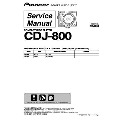
Pioneer Cdj-800 Service Manual 2hbc
December 2019 122
200 Xri Service Manual 1ey27
November 2019 39